About
This project of mine was inspired by Ben Eater and the 8-Bit breadboard computer he made. I would in fact highly recommend you check out his complete video series on it. When I first saw his computer featured on Hackaday I thought it was awesome and immediately wanted to build my own.
But as I started to look into the components needed for the build I figured that it was kind of expensive. And building the computer on breadboards with logic chips would take up a lot of space, bring up problems with bad connections, etc … So instead I thought I could just make the computer in an FPGA(plus I wanted to get into FPGAs anyway). This way I could learn some stuff about working with FPGAs while making the 8-bit computer.
Well … as it turns out the FPGA dev board wasn’t that cheap either and debugging the FPGA designs can be kind of a pain as you don’t have easy access to the connections. So using an FPGA definitely has its drawbacks. Like … not having a cool looking breadboard computer at the end. For this reasson I might actually build an actual breadboard computer at some point in the future. But nonetheless, this whole thing was a great learning experience.
Despite using an FPGA I purposefully didn’t use HDL but made the computer by using discrete logic gates. I also mostly didn’t use any of the premade components in Quartus(FPGA development environment). If I had used HDL or the prebuilt components(flip flops, muxers, …) it would have been easier but I wouldn’t get to understand how a computer works at the logic gate level. This way it was way clearer to me how a computer is built and how it operates.
Project Files
Hardware used
- #adAmazon LinkDE0 Nano – Altera Cyclone IV FPGA development board
- #adAmazon LinkArduino Mega
- #adAmazon LinkArduino Nano x2
- #adAmazon LinkSSD1306 OLED Screen x2
- #adAmazon LinkLogic Level Converters
- #adAmazon LinkBreadboards
- #adAmazon LinkButtons
- #adAmazon LinkLEDs
- #adAmazon LinkResistors
- #adAmazon LinkWires
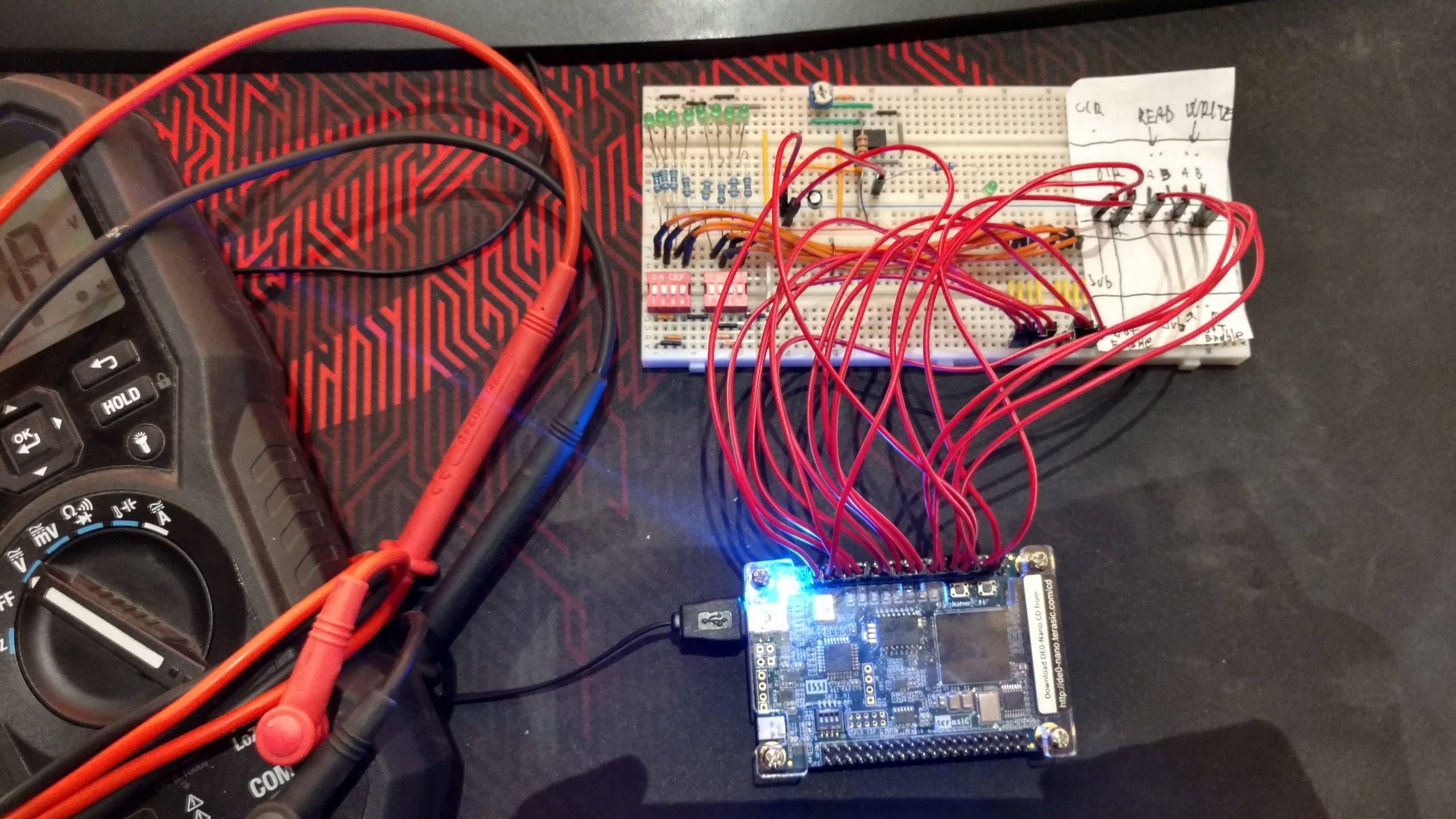
Hardware Connections
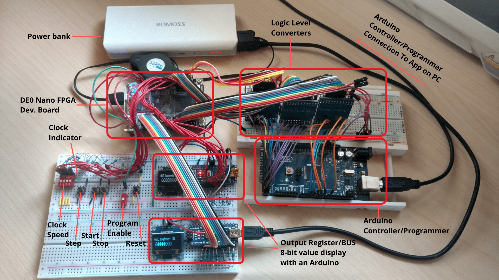
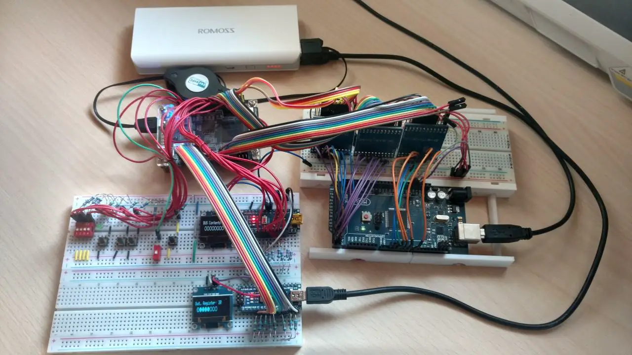
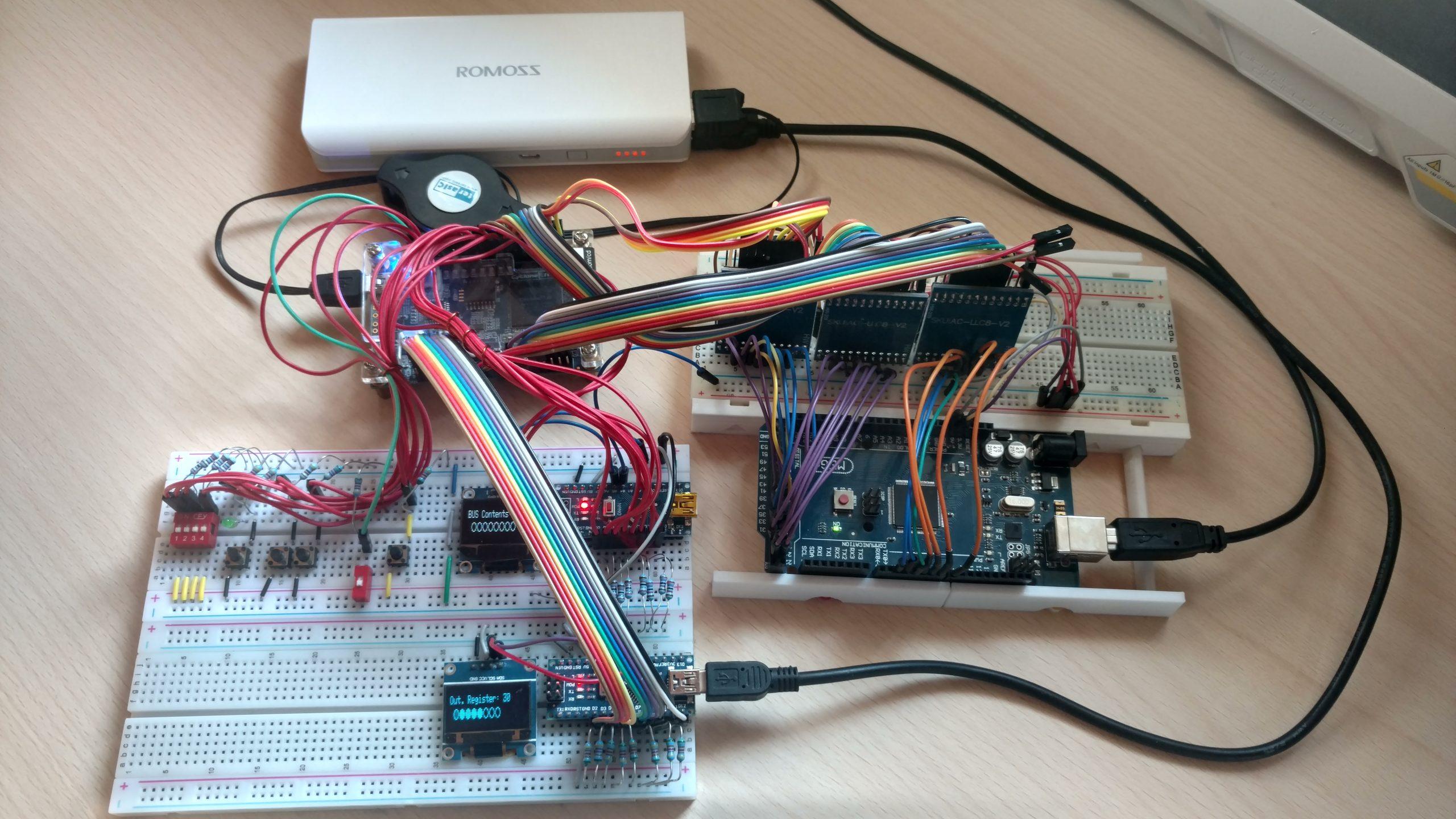
- The FPGA development board contains the computer itself and it gets powered from the power bank above it.
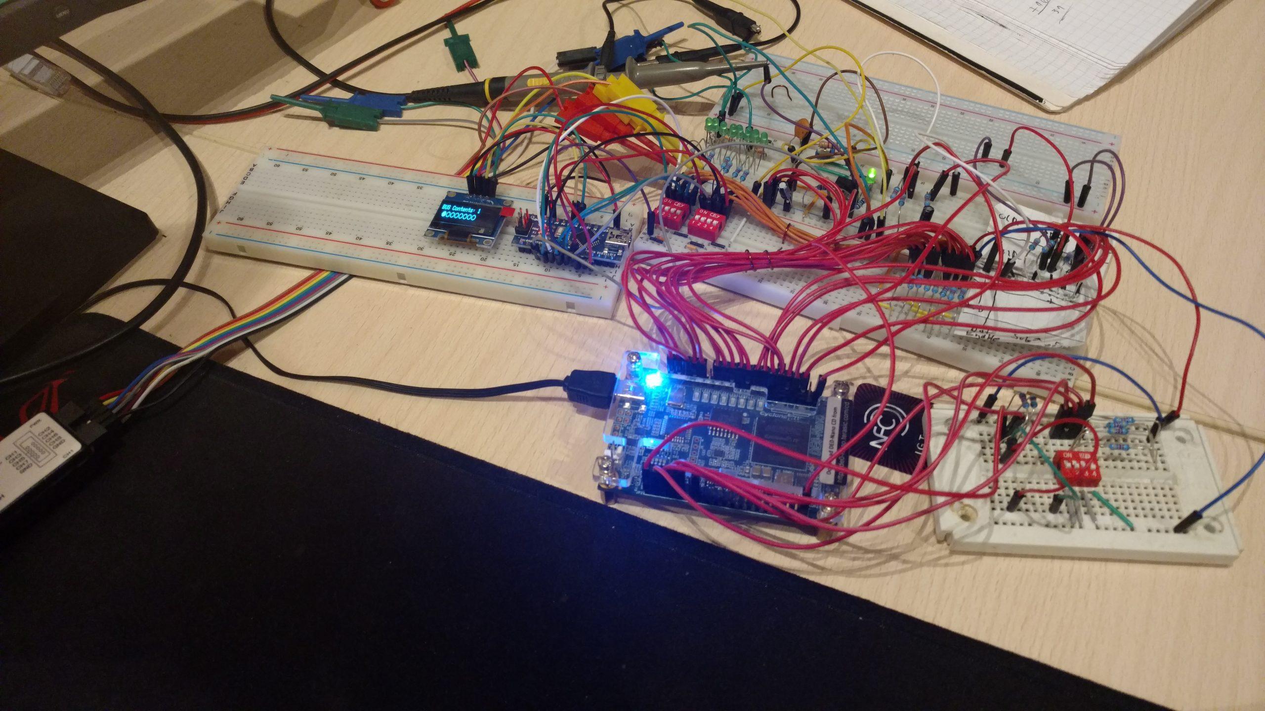
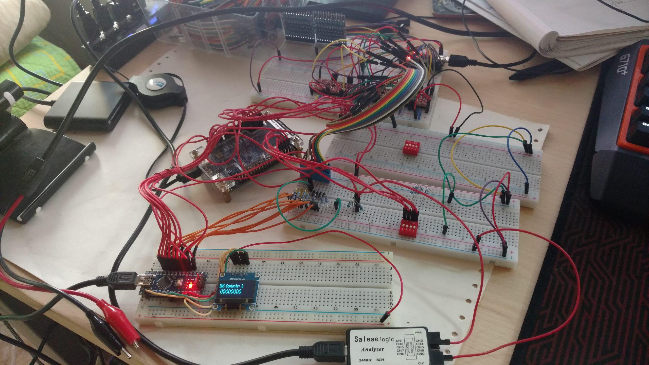
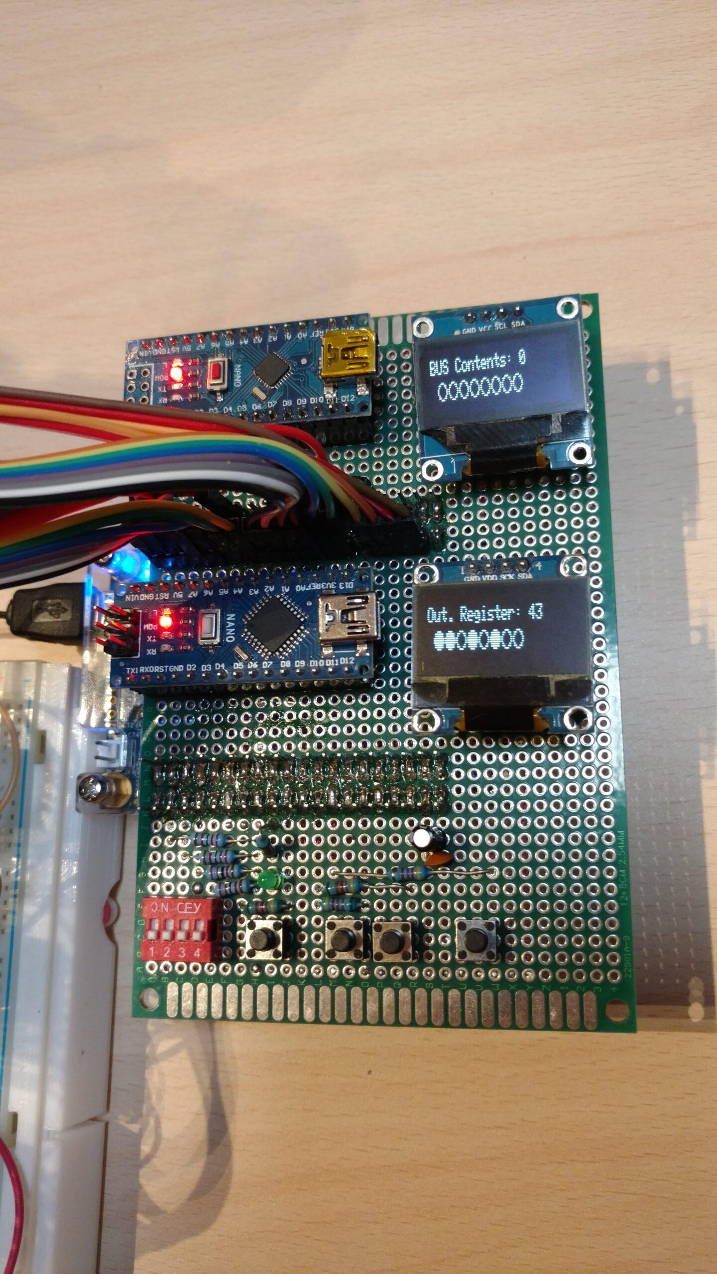
- The two Arduino minis just take the binary logic levels from the wires and display the value in decimal on an I2C SSD1306 OLED screen. They replace the LEDs and at the same time conveniently display the decimal value. You can still see the individual binary value represented by the circle at the bottom. I did this instead of using LEDs and/or a 7-segment display because it is more compact and it was easier and more convenient for me to make. Also, the Arduinos are powered separately(from the power bank) and thus don’t draw any current from the FPGA, unlike LEDs. I could’ve used some transistors to drive the LEDs but I think that would’ve looked kind of messy. The upper display shows the contents of the main bus while the bottom display shows the contents of the output register.
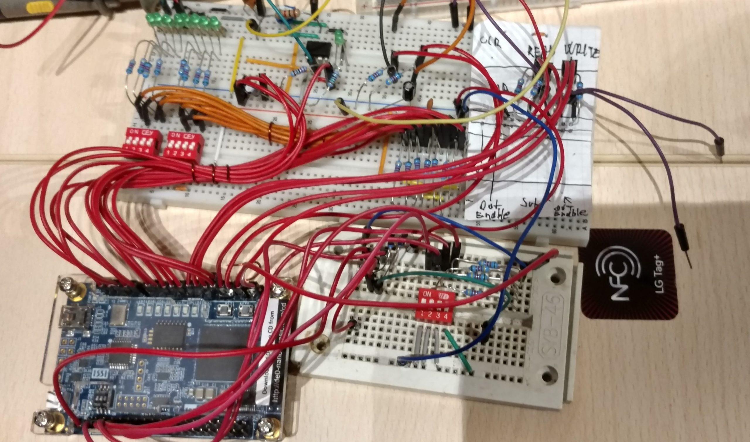
- On the breadboard, you can see all of the controls for the computer. Program Enable is not used with the current Arduino programmer. The DIP switch is used to select one of the 16 clock speeds.
- The logic level converters are used to convert the 5V signals from the Arduino to the 3.3V signals required for the FPGA.
- The Arduino Mega is used as a controller and a programmer. The computer can either be controlled by the buttons on the breadboard or from the application on the PC via the Arduino. The “software” or assembly can be written in the application on the PC and then loaded into the computer via the Arduino. The Arduino is connected to the 8-bit computers RAM and can load data straight into it.
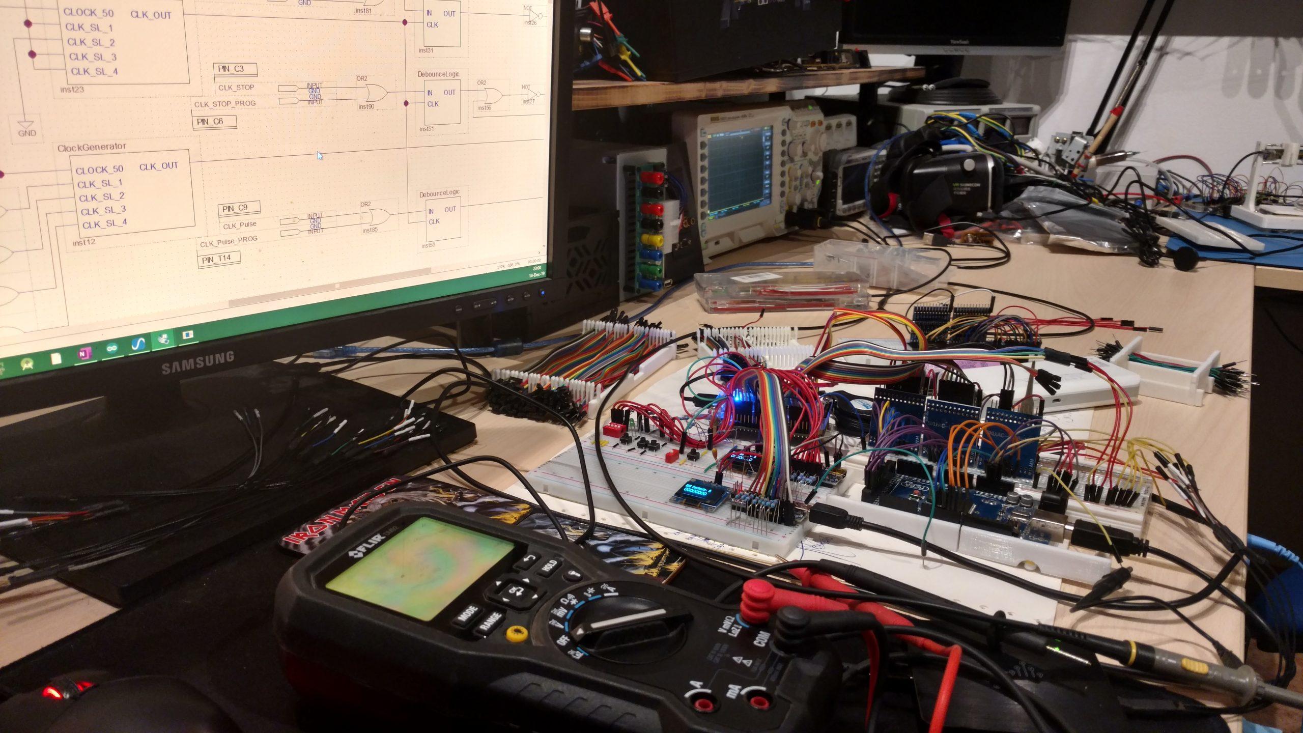
Digital Logic Design

Here you can see the top level design of the whole computer. However in this post I won’t go over the construction of every component. If you are interseted in that see the section with links to indivinual post bellow.
Some Differences compared to a Breadboard computer
Unlike with a breadboard computer where you would use DIP TTL logic chips for the RAM, ALU, Registers, … I had the ability to make all the components from scratch. Here are some of the most notable differences:
- Instead of using DIP switches for programming, my computer has an Arduino interface with an app on the PC(This could actually be used with a breadboard computer too.).
- Everything is assembled from scratch. For example, flip-flops, which then make registers that in turn are used to make the RAM, the program counter was made by multiple ripple carry counters, …
- The RAM and the control unit use a decoder built from scratch. In contrast, Ben used an EEPROM to do the instruction decoding which is a great way to avoid having a mess of wires on the breadboard. For me, however, it was easier to just implement the decoder logic.
- Instead of using 7 segment displays and LEDs to display the output register and bus content, I used an Arduino with an OLED display is used.
- The clock is taken from a 50MHz crystal oscillator present on the FPGA dev. board. It is then divided using a PLL to get a lower frequency. Finally, I then use daisy-chained ripple-carry counters to perform the final frequency division. I then tap off the different frequencies from the different outputs of the ripple carry counters.
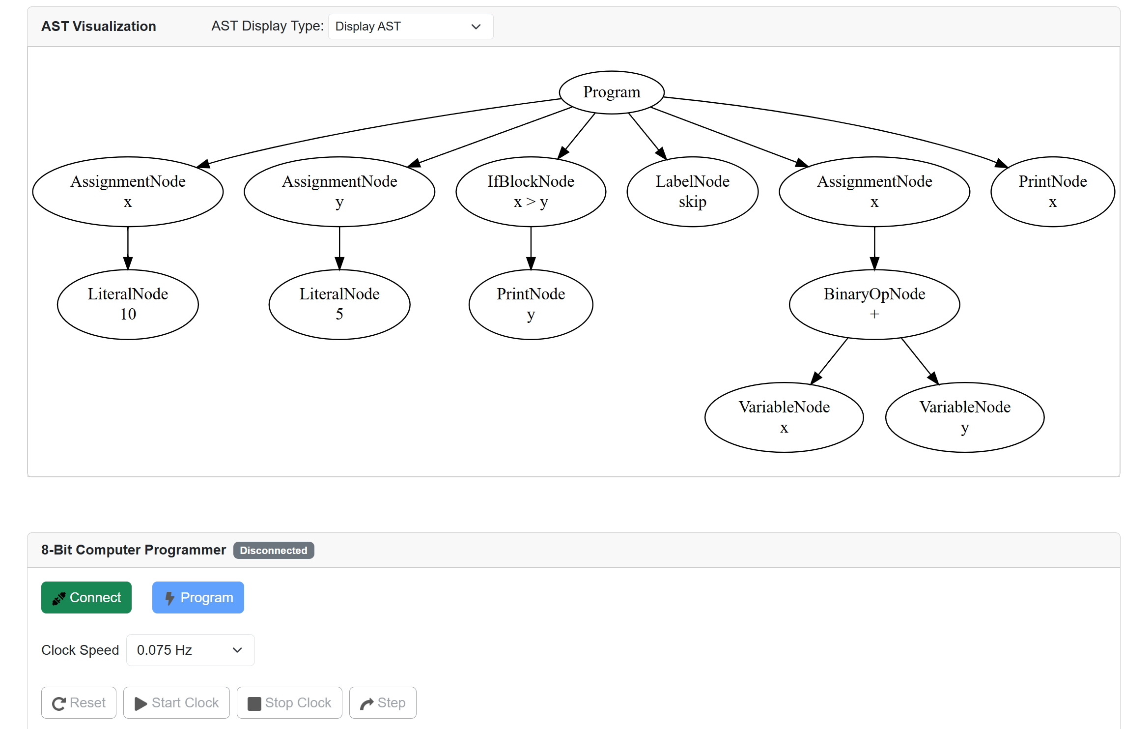
Programming
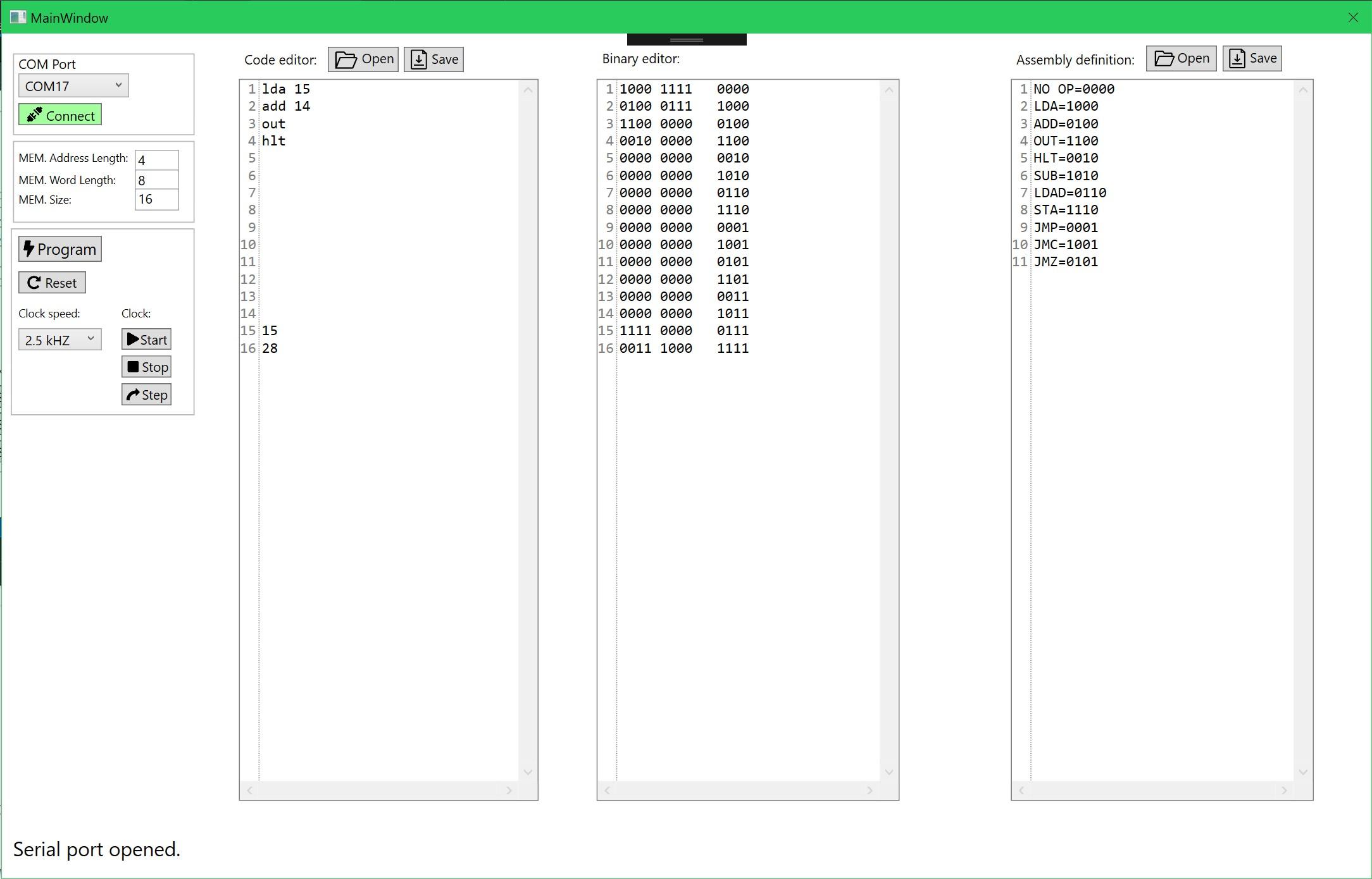
To make programming the computer easier I made this “IDE”. In the first code editor, you write your assembly. In the second one, the machine code gets generated. And in the third one, you can define your assembly(map the assembly to machine code). You can also save/load your assembly program and your assembly definition.
On the left, you have the controls column. At the very top, you can establish a COM port connection to the Arduino.
Then you have the option to set your RAM size, RAM word length, and the memory address length. Currently, this is fixed and can’t be changed. I didn’t really need the option for a bigger memory so I skipped implementing this feature(might add it in the future).
Finally, there are the controls that allow you to control the computer straight from the application/”IDE” on the PC. These controls have the same functionality as the ones on the breadboard.
Programming the computer this way is much faster and easier than using dip switches and manually setting the contents of each RAM address. Especially when I was debugging something and the FPGA had to be reconfigured meaning the computer lost everything in RAM.
See more info about the Arduino programmer here(code and how it works in more detail).
Update:
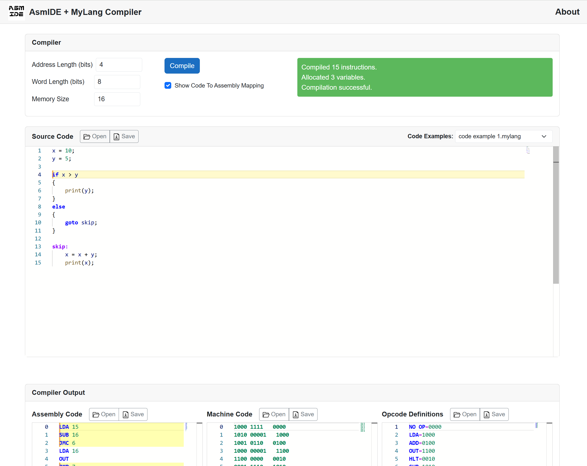
I have ported AsmIDE into a Blazor web app, including a custom compiler I made. For a while, I wanted to make my own compiler for fun and learning. Initially, I was going to make a C compiler, but then I thought it would be nice if I actually made a simple compiler for the 8-bit computer I made.
You can access the web app here: AsmIDE + MyLang Compiler
See more about the compiler itself in this blog post here.
Debugging The Designs In The FPGA
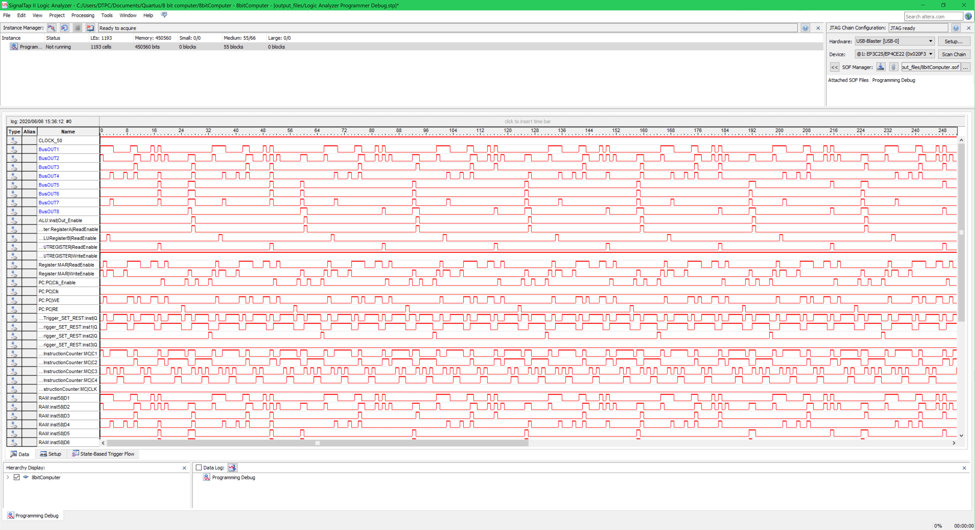
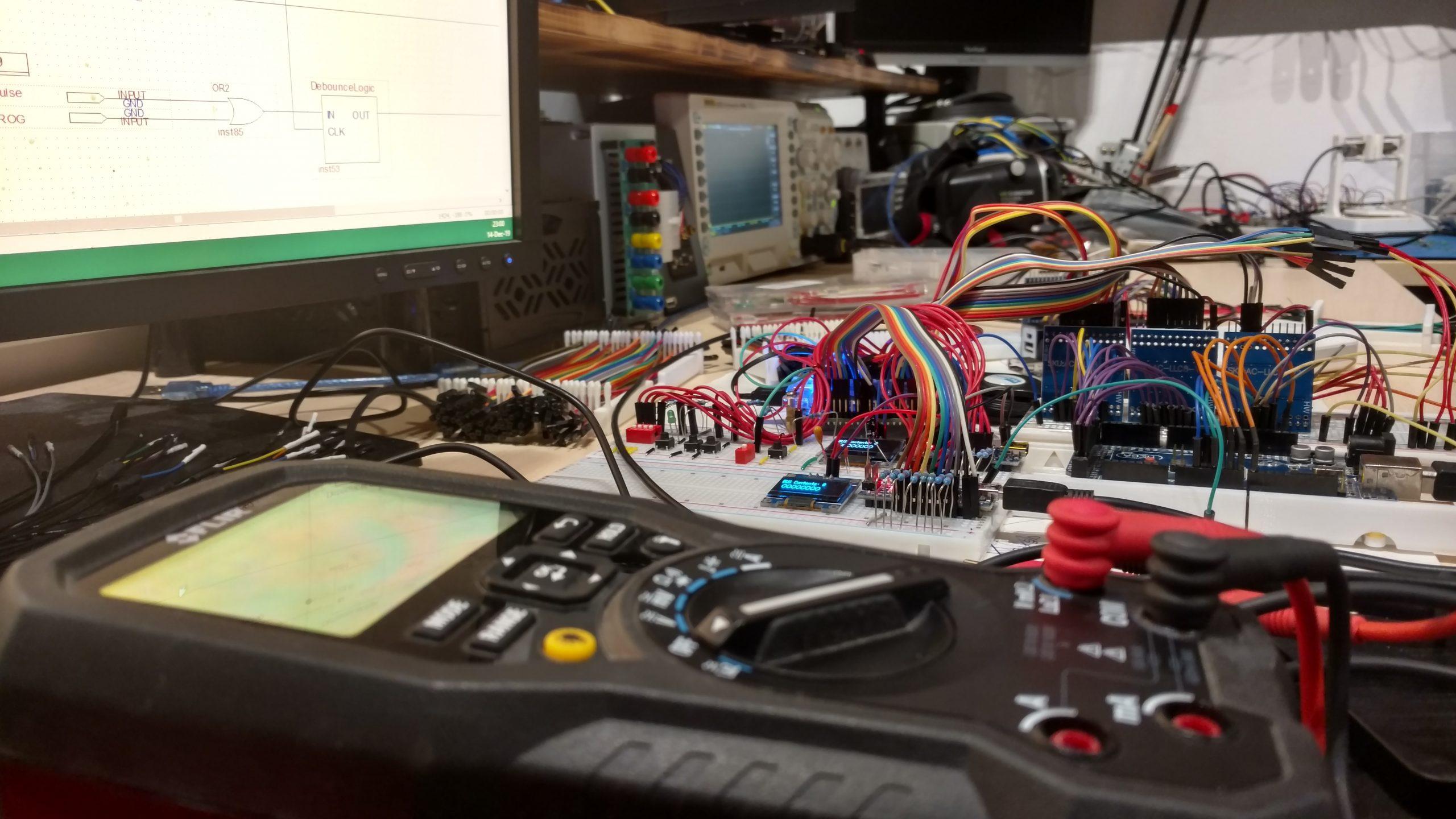
The debugging can be a bit difficult in an FPGA compared to a breadboard where you can just use a multimeter/oscilloscope to probe your signals anywhere and at anytime. With the FPGA you have to connect the point you want to monitor to a pin first, re-compile, reprogram the FPGA and then you can measure the value. However, Quartus does have a very useful tool called signal tap logic analyzer. This is a logic analyzer that gets embedded in your FPGA(it will occupy some space) and provides you with the values in the Quartus IDE.
Demonstration
Topics In More Detail
Build Progress


Hello! Hope you are doing well.
I am a student at Madison College in Wisconsin, and I would like to use your project as inspiration for an Honor Project.
I will be honored if you give me permission to do so.
Hi.
You can use, modify or copy anything you want. No problem.
I’m glad my project was useful to you.
Hello! Hope you are doing well.
I am a student at Madison College in Wisconsin, and I would like to use your project as inspiration for an Honor Project.
I will be honored if you give me permission to do so.
Sincerely,