Home

About
In this post, we’ll take a look at the clock module of my 8-bit computer. Ben used a 555 timer in his clock module to generate the clock signal for his breadboard computer. The approach I took is a bit different.
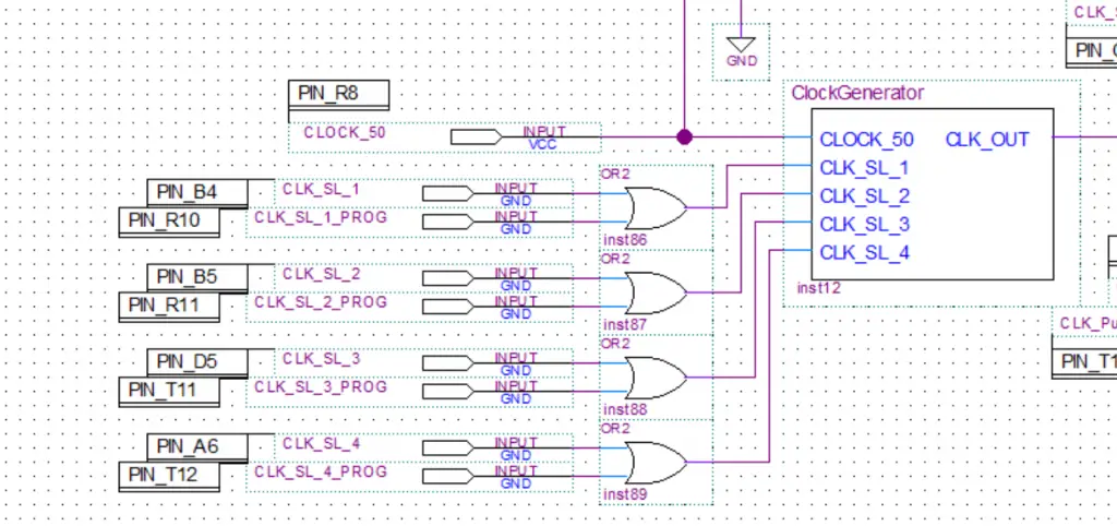
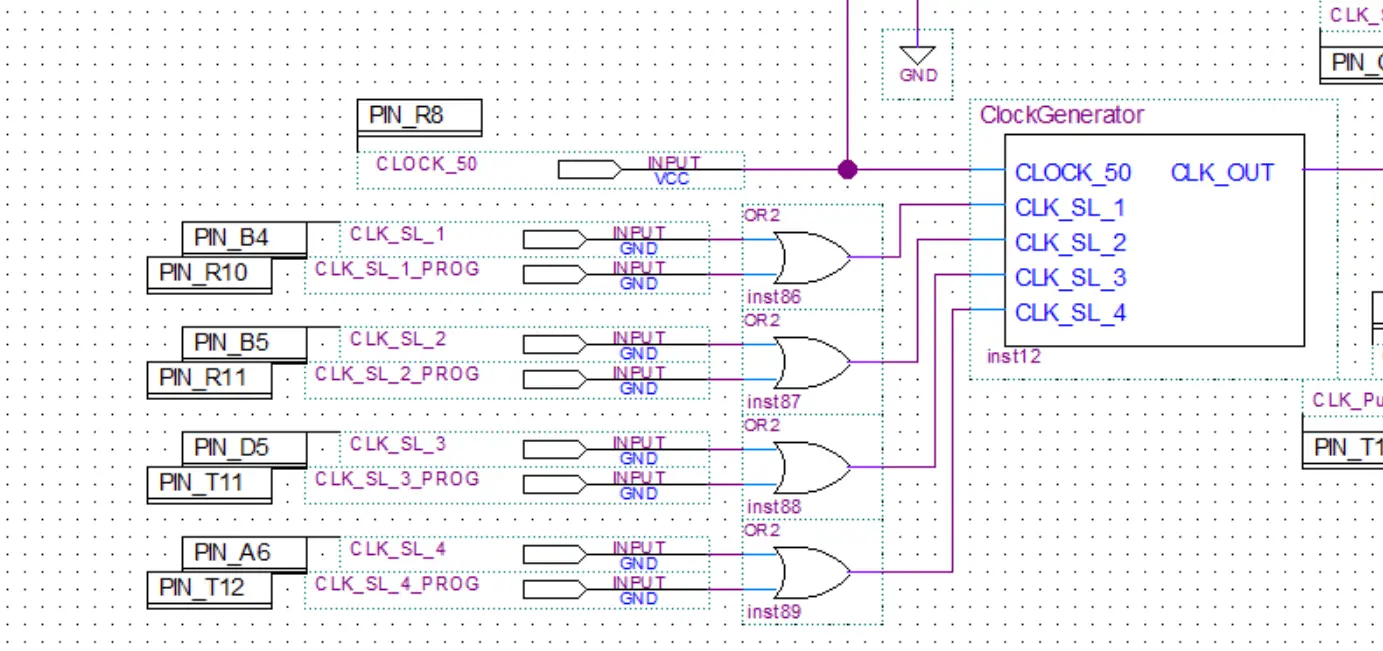
The DE0 Nano FPGA development board has an onboard 50 MHz crystal oscillator connected to one of the pins of the FPGA. This is where we can get our clock signal from. The problem is that the frequency is way too high for the computer and needs to be lowered. This can be accomplished by dividing the frequency using a frequency divider(which is esentially just a ripple-carry counter) or by using a PLL(phase locked loop).
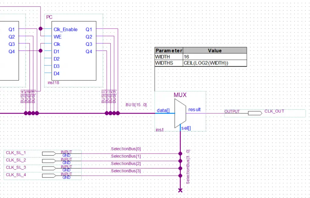
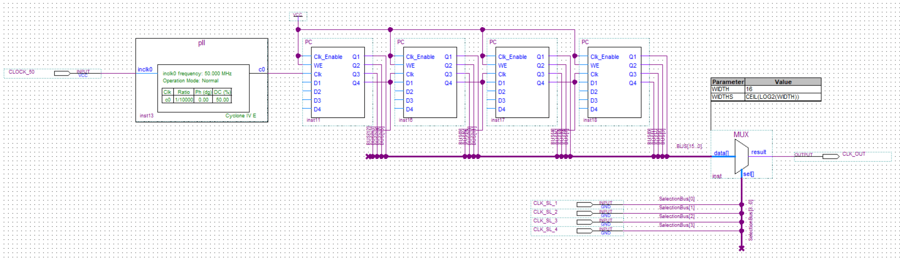
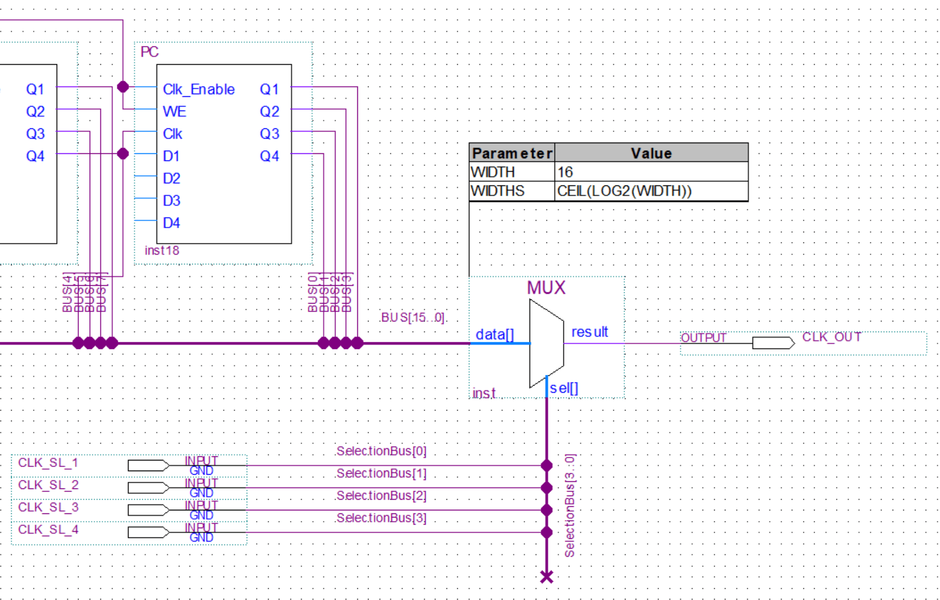
First I used a PLL to lower the frequnecy. Then I used multiple dividers with varying numbers of od division stages to get different frequencies. Finally a multiplexer was used to enable the selection of the desired frequency.
Frequency divider
First the 50 MHz input from the crystall oscilator is lowerd using a PLL. I won’t go into details about PLLs here(I’ll make a separate post just about them some time in the future).
Then the signal is feed into the PCs for further division. The program counter is in essence just a ripple-carry counter so I ended up reusing it as a frequency divider.
About
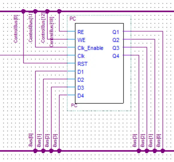
In this post, we’ll take a look at the program counter of my 8-bit computer. The PC(program counter) is used to store the memory address of the next instruction to be executed. After the instruction was executed it the value in the PC will be incremented by one, therefore, pointing at the next memory address that contains the next instruction.
The PC is almost identical in construction to the microinstruction counter as both of them are just ripple-carry counters.
Differences:
- The PC has the ability to read in a value as opposed to just being able to increment the existing one. This is what enables the JMP instruction.
- The PC has tristate buffers to control the outputs(because it is connected straight to the bus). Meanwhile, the microinstruction counter is always outputting its value.
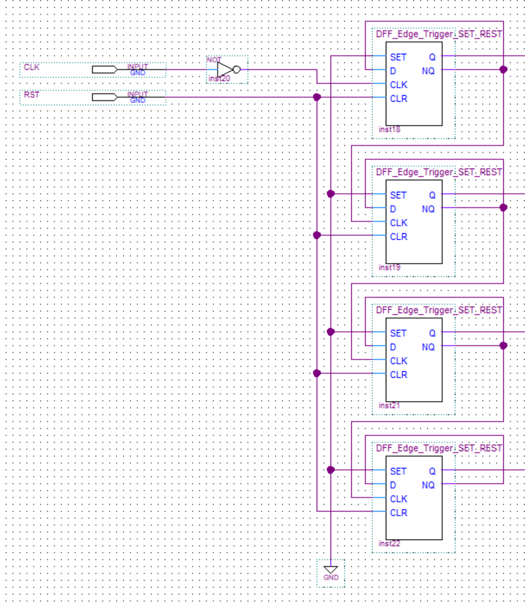
Note: A ripple-carry counter is an asynchronous counter because only the first flip-flop is connected to the clock. All others will receive their clock signals from the output of the preceding flip-flop.
Ripple Carry Counter
I made the ripple-carry counter by chain together D flip-flops. On each one, the NQ output needs to be connected to the D input of the same flip-flop. Meanwhile, the Q output of the first flip-flop needs to be connected to the clock input of the next one. This pattern can continue for as many bits as you need.
Having the DFFs connected in this way will give us the desired effect of toggling the stored value each time a clock pulse is received.
In the image below, you can see the ripple carry counter in the microinstruction counter.
A counter can also be made from other types of flip-flops. Here is an interactive example of a counter made from JK flip-flops.
Program Counter

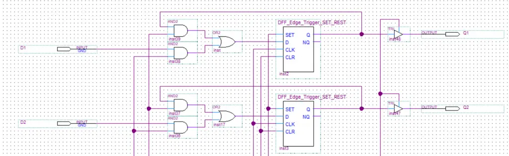
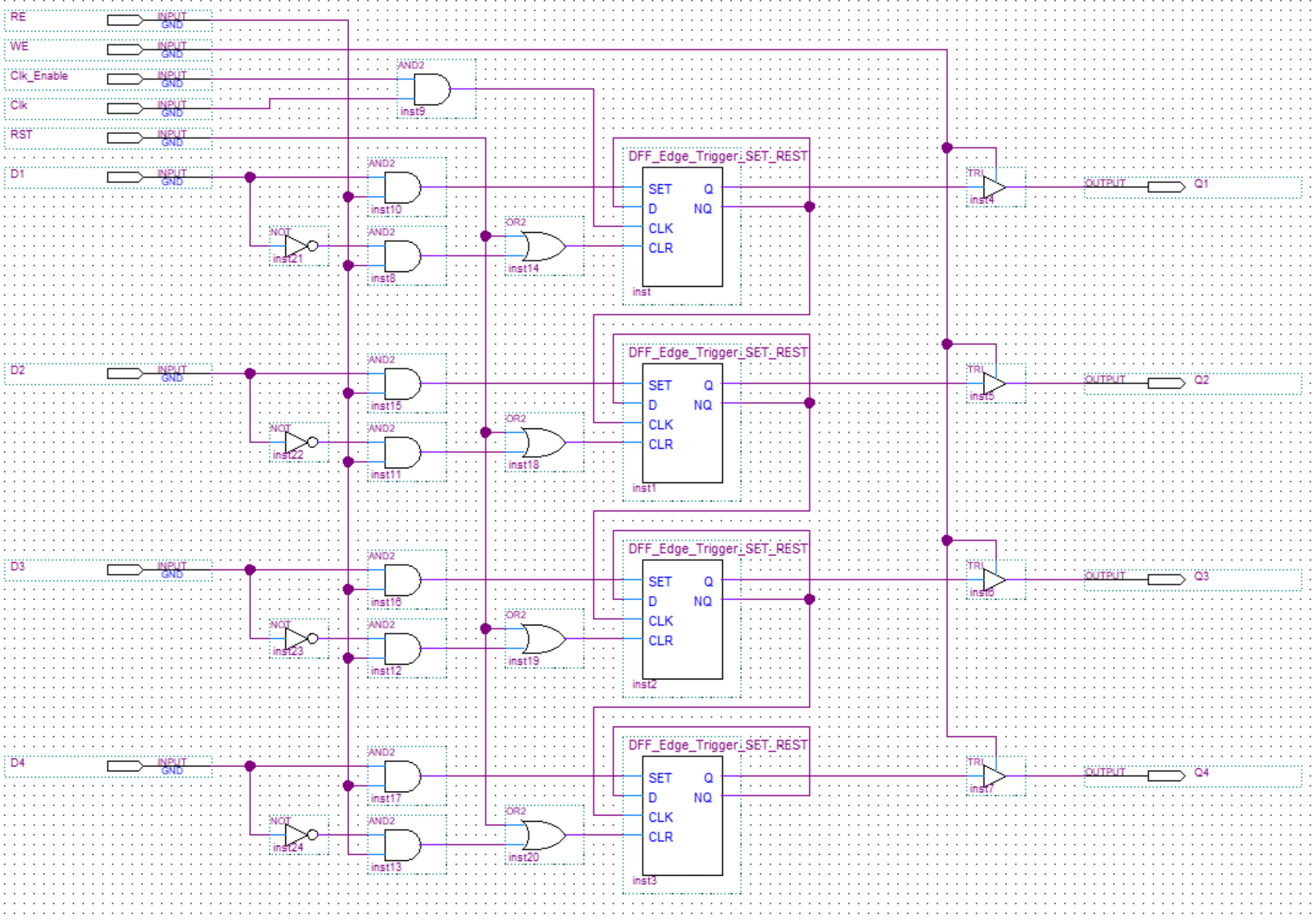
As already mentioned the program counter has tristate gates controlling its outputs and the ability to read in a value.
This is how the read enable circuits works: if read enable is high one of two things can happen:
- If the input bit(D1 for example) is a 1 the first AND gate will output a 1 and activate the SET input on the flip-flop setting its stored value to 1.
- If the input bit is 0 the second AND gate will output a 1 and activate the CLR input on the flip-flop setting its stored value to 0.
About
In this post, we’ll take a look at the control unit of my 8-bit computer. Ben used an EEPROM to make the control unit in his computer. This is a quite clever approach if you are building your computer on a breadboard as it drastically decreases the complexity, amount of components and space needed. But in my case, it was much easier to just implement the control unit using discrete logic gates.
The job of the control unit is to take in an instruction decode it and execute it by toggling the control lines to various components in the appropriate sequence.
Note: The images don’t include the whole circuits as they are too big. The circuitry just repeats anyway so you are not missing out on anything.
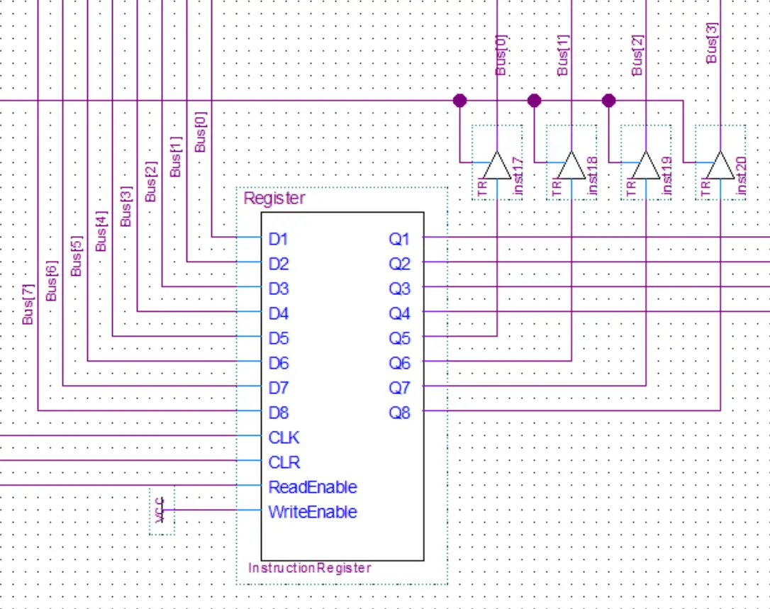
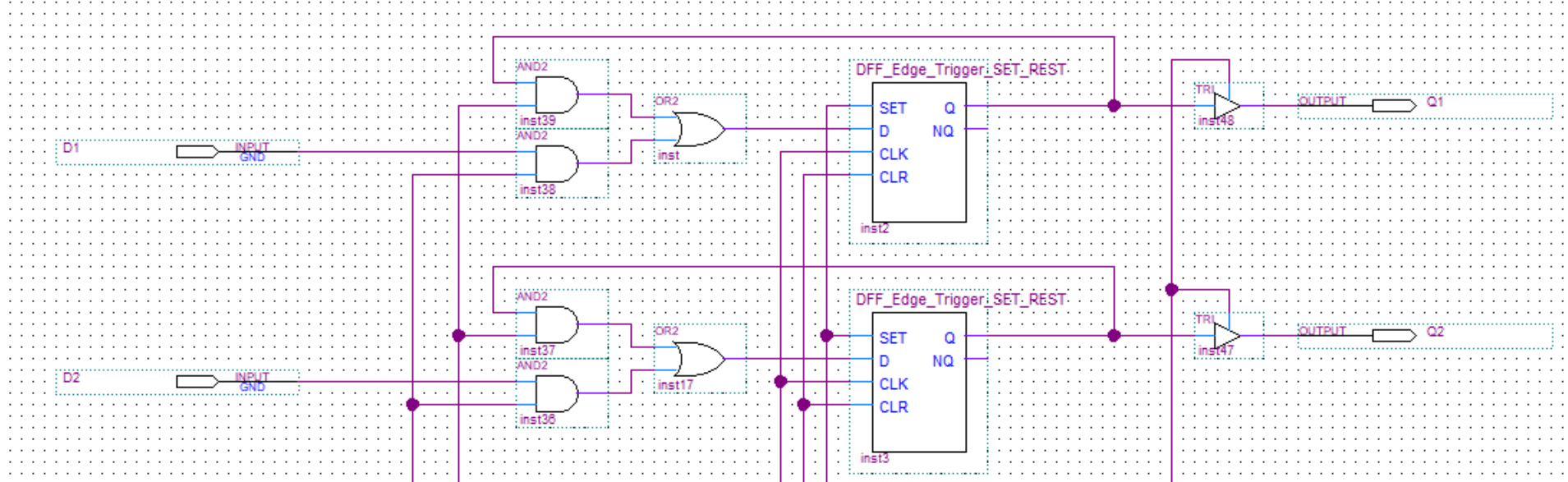
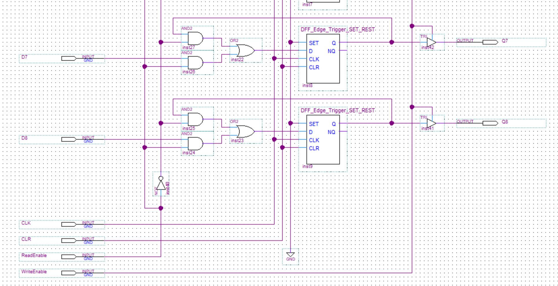
Instruction Register
The instruction register as the name implies is used to store the current instruction and forward it to the control unit to be decoded. It will read 8 bits from the bus. Once the values have been read into the register it will output 4 of those bits (the instruction part) to the control unit to be decoded. While the other 4 bits(the value) will be output back to the bus.
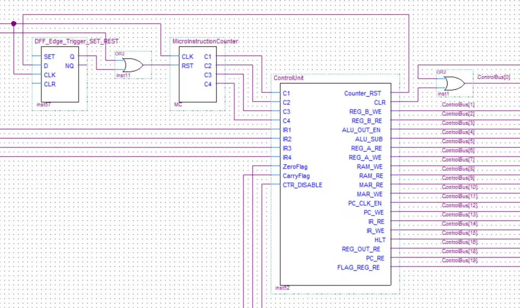
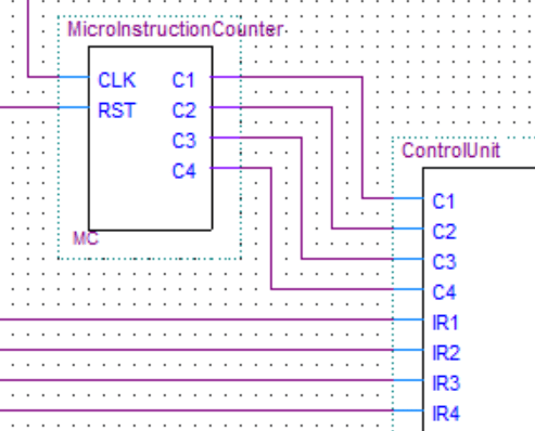
Control Unit
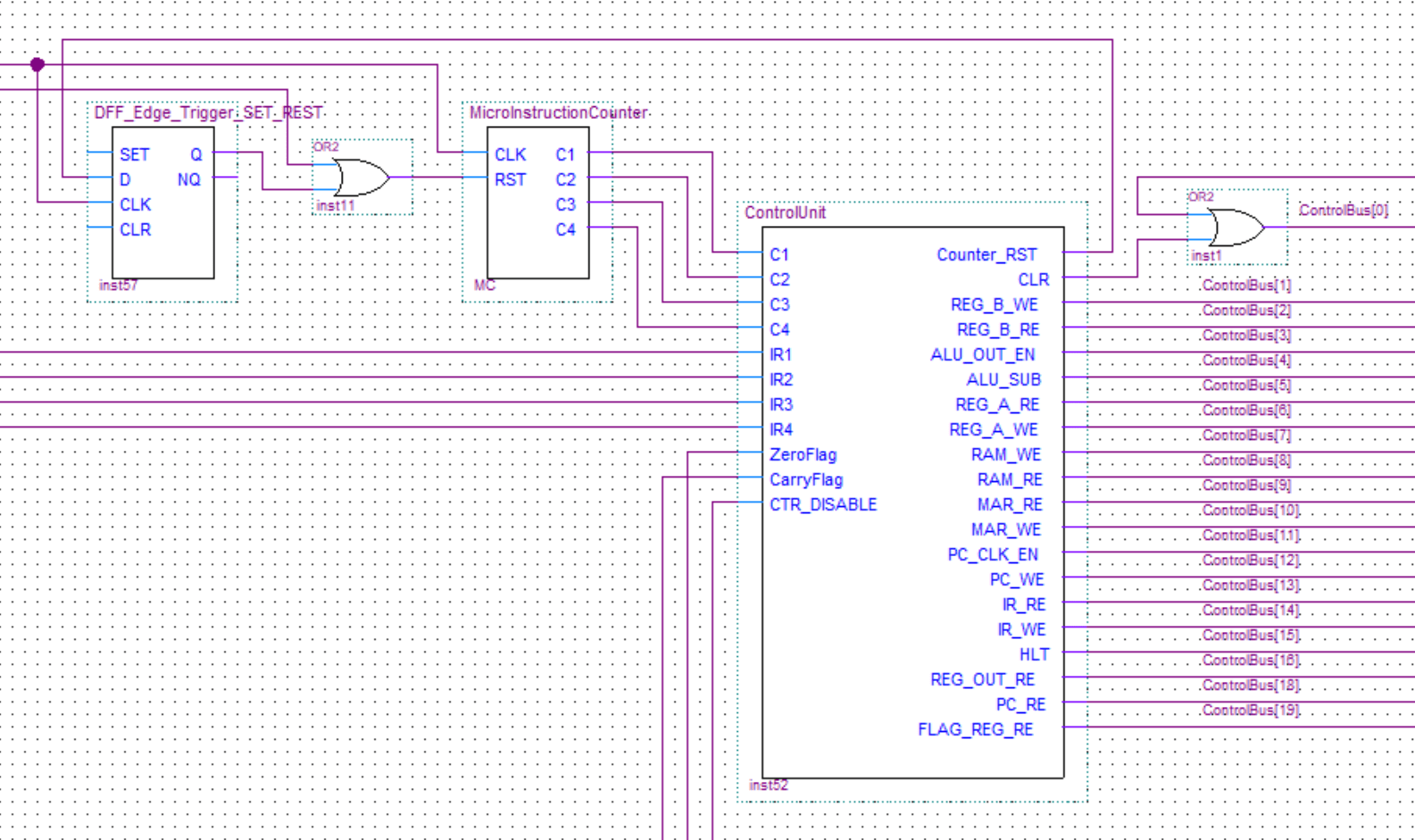
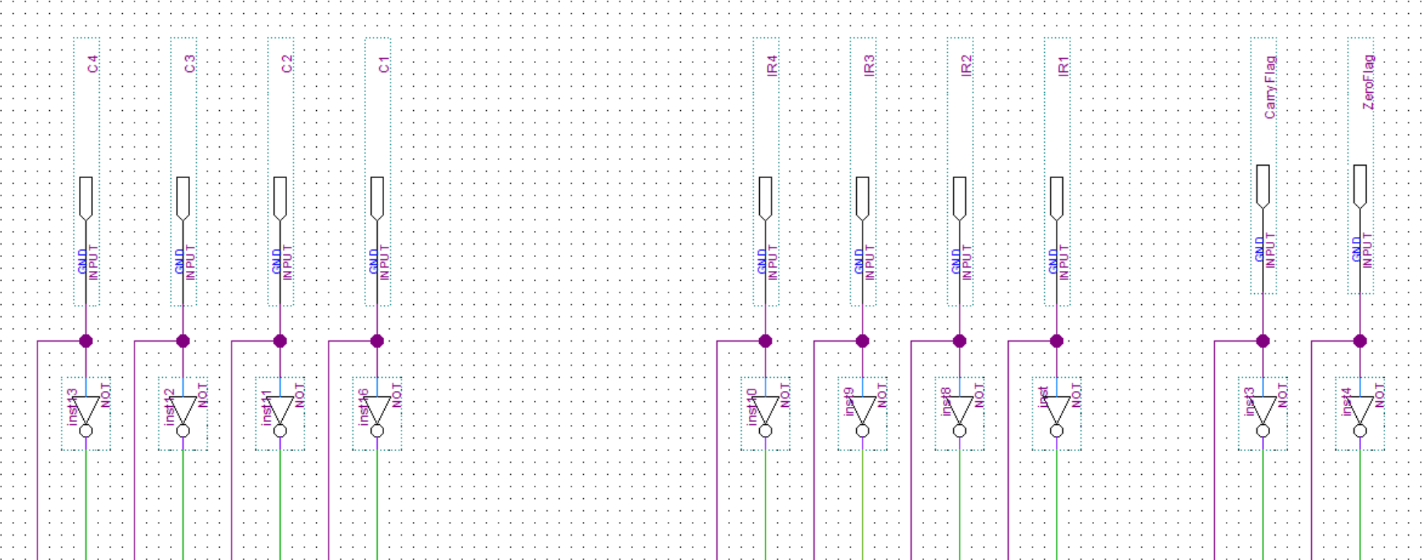
Here you can see the inputs coming into the control unit from the instruction register, flags register, and the microinstruction counter.
The microinstruction counter is just a ripple-carry counter(same as the program counter). It is used to step through all the single actions actually required to execute an instruction.
The flags register is used to store the flags conditions from the previous operation. This computer has two flags. The zero flag is for when the result of a computation in the ALU is zero. While the Carry flag is for when the computation in the ALU exceeds 255 and carries over/overflows. These flags can then be used to implement the JMC(jump if carry) and JMZ(jump if zero).
Finally, you can also see a bunch of output lines to control all the various components of the computer
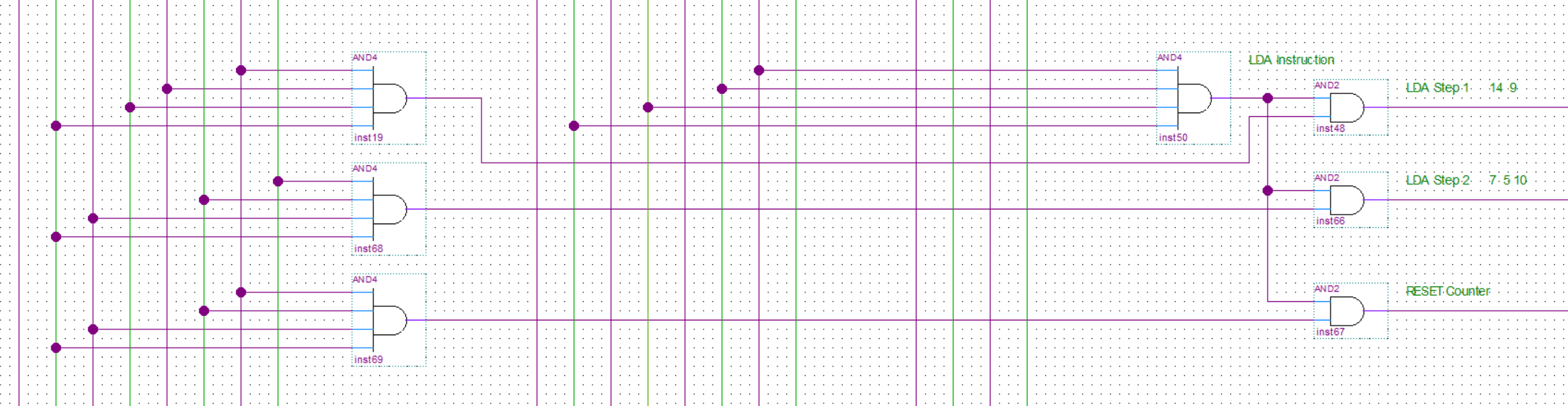
In the first image below, you can see the inputs to the decoder. After that, there are two examples of how the instructions are decoded to the multiple steps(microinstruction) required to execute them.
There are three decoders. First for selecting the instruction(input from the instruction register), second for selecting the step(input from the microinstruction counter) and the third used for the flags in case the instruction requires that like the JMZ and JMC instructions.
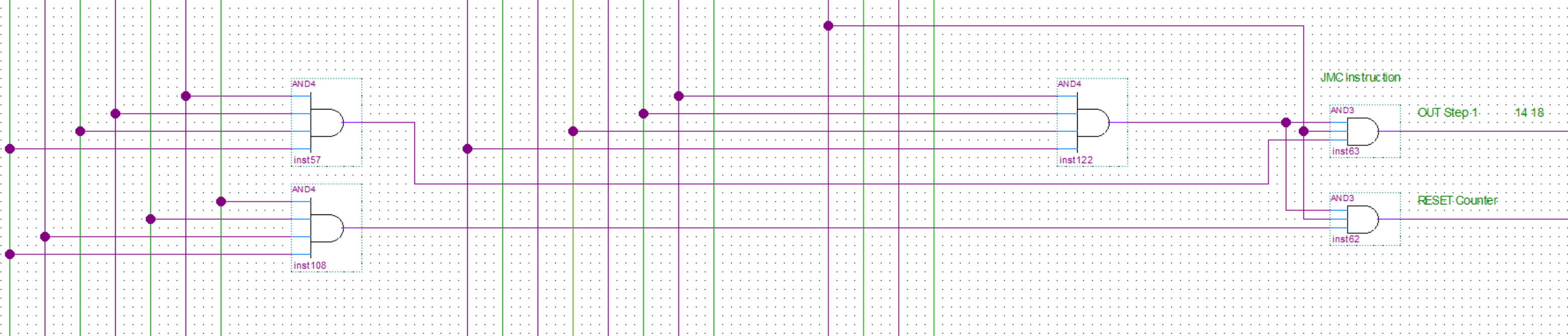
Finally, this is an example of an output. All/most of the outputs have OR gates connected to them to funnel in the signals from all the microinstruction steps that require that particular output. There is also an AND gate at the end so all the outputs can either be enabled or disabled.

About
In this post, I will describe how I implemented the RAM in my 8-bit computer.
The RAM size is very small, 16 cells(words) each one with 8 bits. It’s a small and simple computer so a program and its variables will be directly loaded into memory using a programmer. Results and any temporary variables are also all just stored in RAM. The only exception is if you want to output a value you can directly load it into the output register.
Note: The images don’t include the whole circuits as they are too big. The circuitry just repeats anyway so you are not missing out on anything.
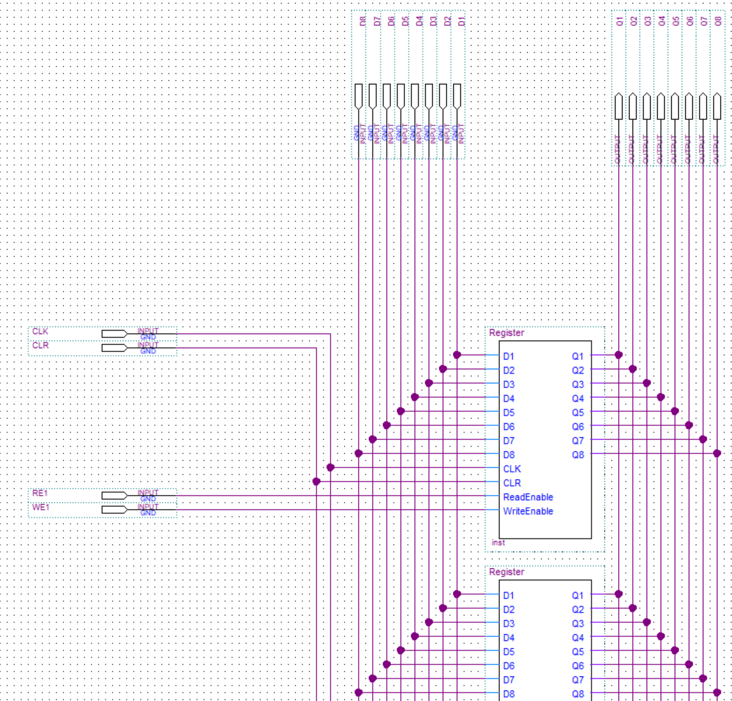
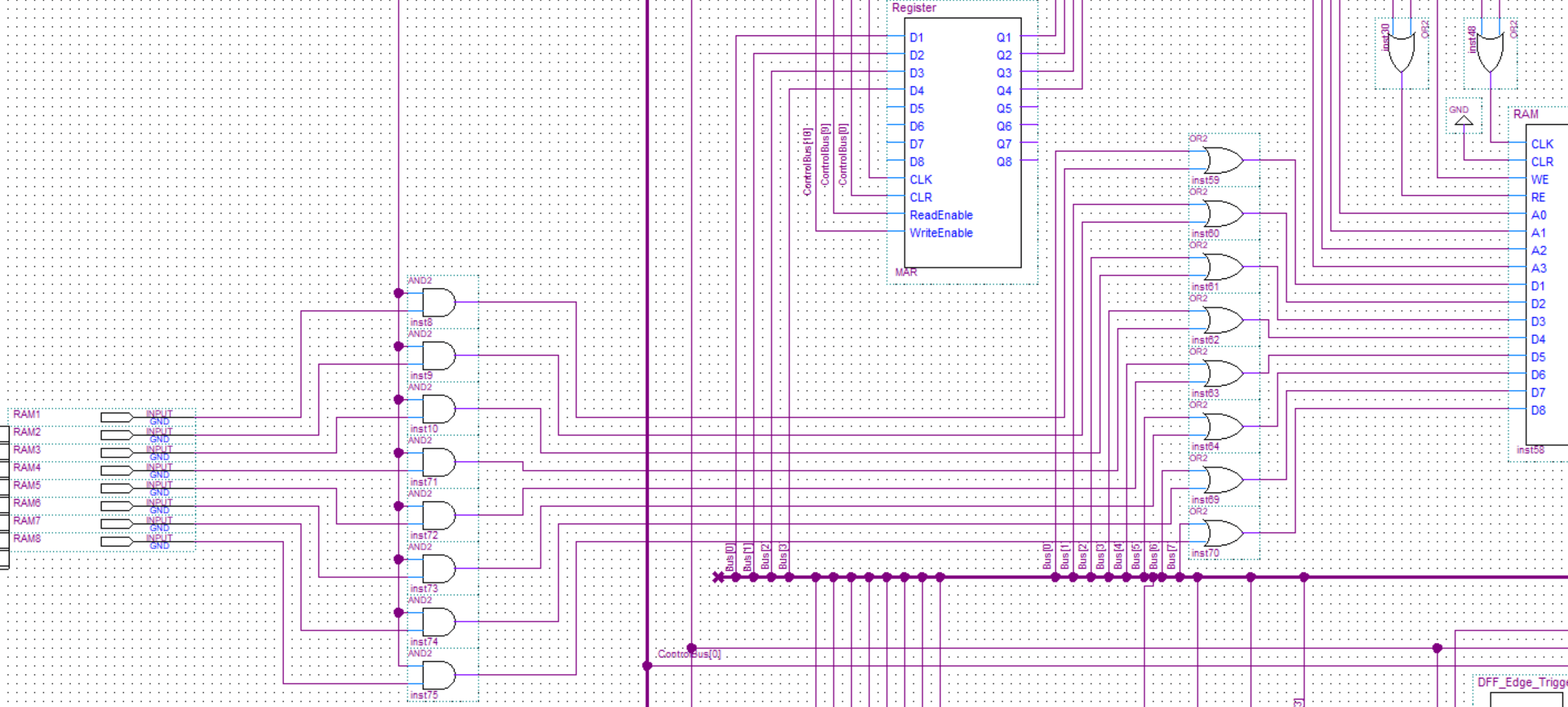
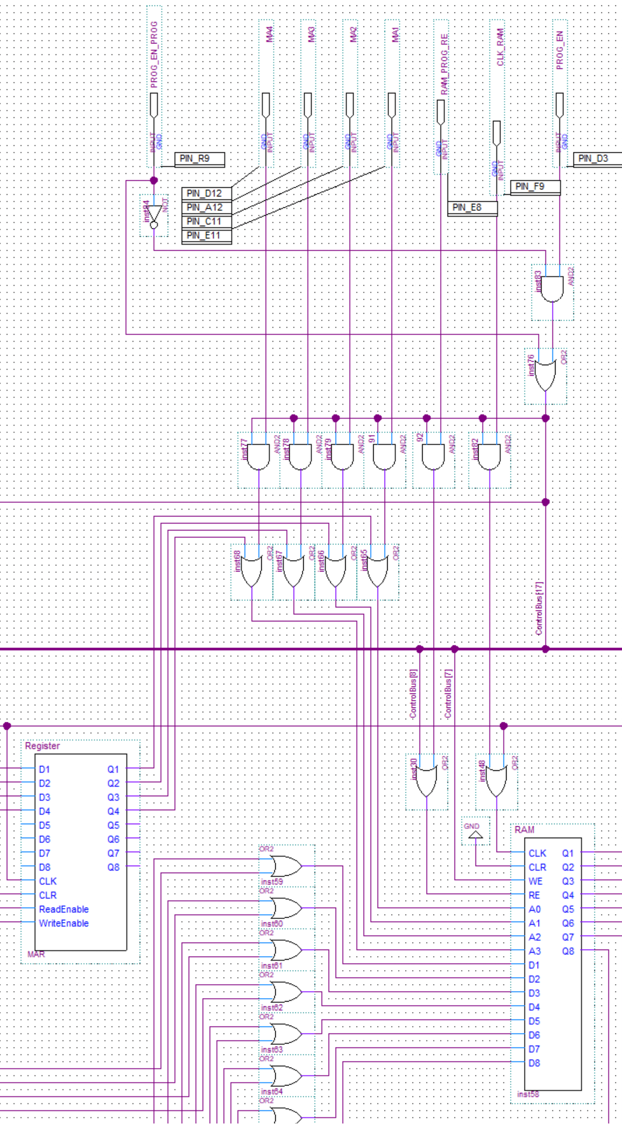
MAR(memory address register)
Before a RAM read or write operation is about to be executed the memory address has to be stored into the MAR. Then when the read or write is performed the MAR will provide the RAM with the memory address location.

RAM(random access memory)
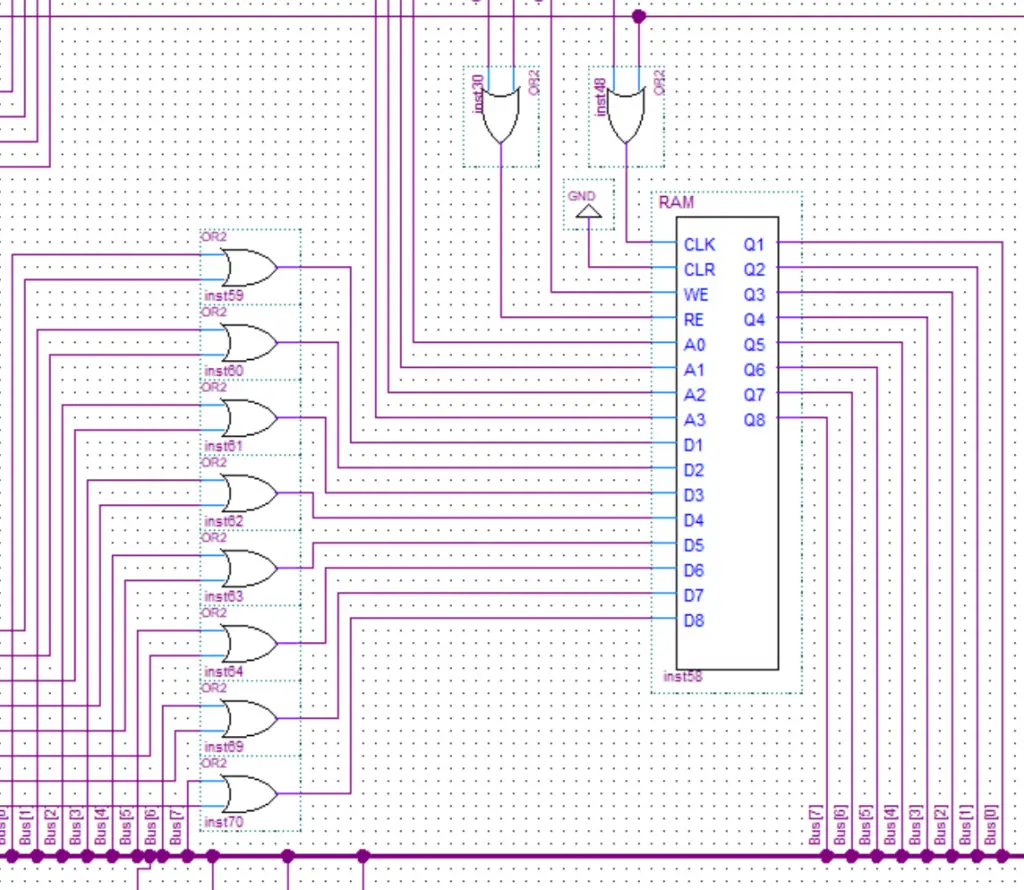
The RAM is connected to the bus via 8 inputs and 8 outputs(one for every bit of the 8-bit computer). The clock, read and the data inputs all have two possible sources. One is from the computer itself while the other is from the Arduino programmer that will put the data into the RAM.
The RAM module will take in the signals to read from RAM, write into RAM, and memory address location. It also takes in the clock signal and the clear memory signal which get forwarded to the RAM cells module. The memory address first gets decoded using a decoder. Then we determine whether to read or write to that address. Finally, the signal gets sent to the appropriate input on the RAM Cells module.

RAM Cells
The RAM cells are made from registers(see how the registers are made here). The clock and clear lines of all the registers are tied together. All of the inputs/outputs are connected to an input/output BUS.
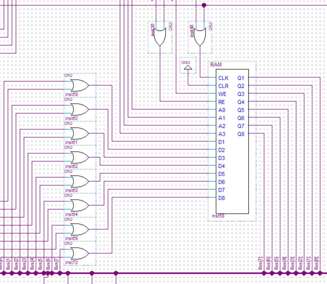
Loading data into RAM
In this image you can see the RAM data input coming from the programmer. First the data lines go through some AND gates which act as an enable/disable. Before going into the RAM the inputs from the programmer and the bus are joined together using OR gates.
In this second image you can see the inputs for the memory address, RAM clock, RAM read enable and program enable. Same as before all the inputs go through AND which are used to enable/disable the inputs from the programmer. Finally the inputs from the programmer and the inputs from the computer are joined using OR gates and then fed into the RAM.
About
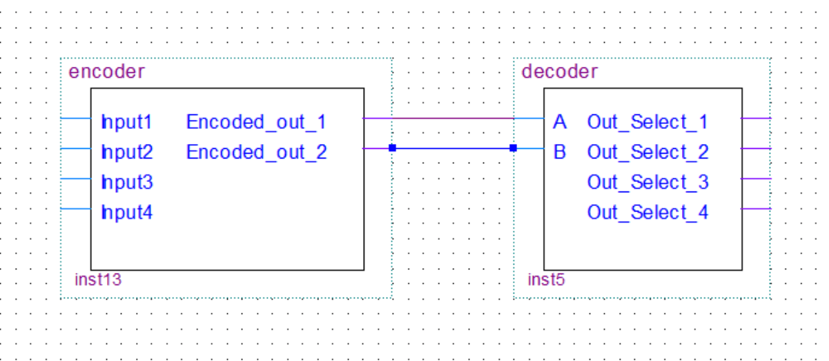
In my 8-bit computer build, I only used decoders. However, I will still cover encoders in this post for the sake of completeness. You can see the decoders being used in the RAM, multiplexers, and the control unit of the computer.
Decoders decode the binary value on the input to an individual selection on the output. The encoder will of course do the exact opposite.
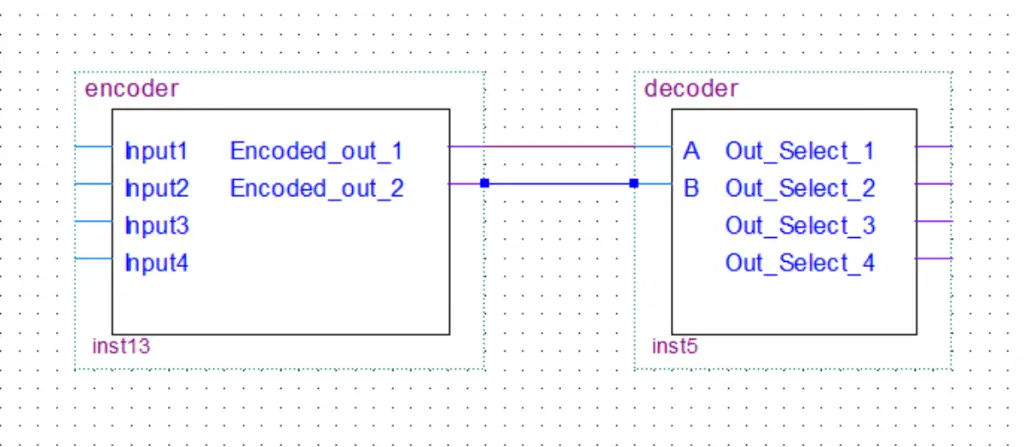
In this post, we’ll take a look at encoders/decoders with 4 inputs/outputs because it’s easier to understand how they work. The logic is the same for more inputs/outputs, the logic circuit just gets scaled up.
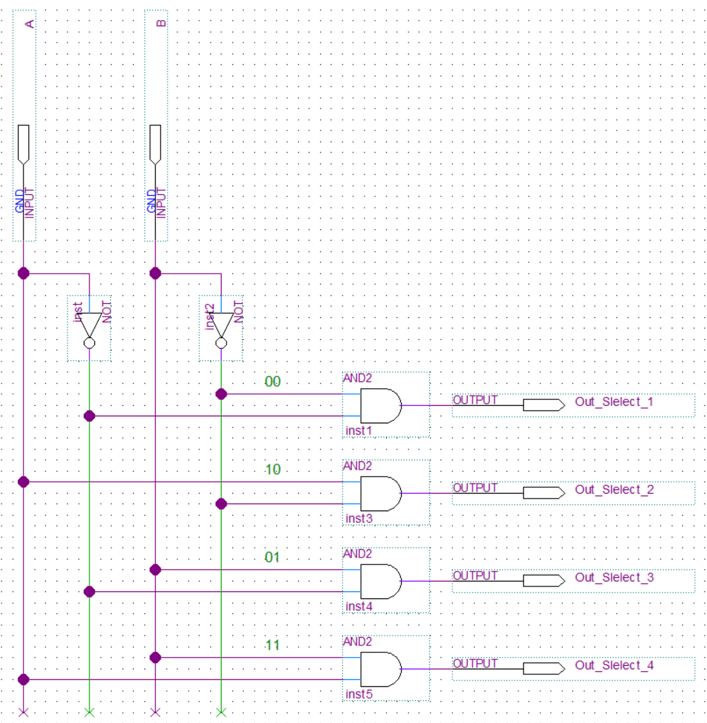
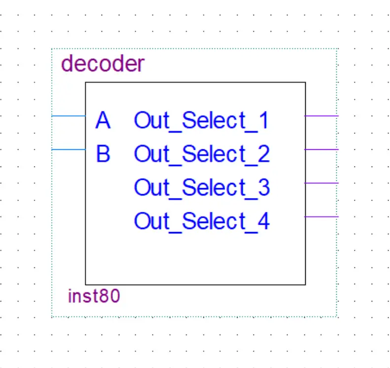
Decoder
In this example, we have a 2 to 4 decoder(described as n to 2n ). The n stands for the number of input lines. This decoder will take 2 input lines in and decode(select an output by setting it high) them to 2n or in this case 4 output lines.
We start out with two inputs(A and B). Because we are dealing with digital logic we have binary values. So two values and two inputs give us four different combinations(00, 10, 01, 11). To be able to represent all the states we add a NOT gate to each input. This way we have all the possible combinations. So for example if we want the first output(Out_Select_1) to be 1 the two inputs to the AND gate have to be connected in such a way that they will both be 1 when A and B are both 0.
The same thing is done for the other outputs but for a different combination.
Truth Table
| A | B | Out_1 | Out_2 | Out_3 | Out_4 |
|---|---|---|---|---|---|
| 0 | 0 | 1 | 0 | 0 | 0 |
| 1 | 0 | 0 | 1 | 0 | 1 |
| 0 | 1 | 0 | 0 | 1 | 0 |
| 1 | 1 | 0 | 0 | 0 | 1 |
Boolean Expression
out_1 = A'.B'
out_2 = A.B'
out_3 = A'.B
out_4 = A.B
out_2 = A.B'
out_3 = A'.B
out_4 = A.B
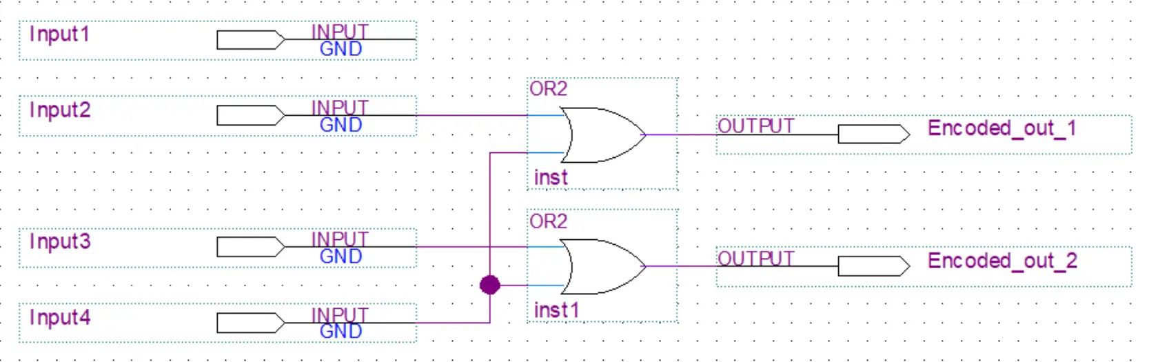
Encoder
The encoder will do the opposite of the decoder. In this example, we have a 4 to 2 encoder(described as 2n to n ). The n stands for the number of output lines. This encoder will take 4 or 2n input lines in and encode them to n or in this case 2 output lines(select an output by setting it high).

Truth table
| Input4 | Input3 | Input2 | Input1 | out_2 | out_1 |
|---|---|---|---|---|---|
| 0 | 0 | 0 | 1 | 0 | 0 |
| 0 | 0 | 1 | 0 | 0 | 1 |
| 0 | 1 | 0 | 0 | 1 | 0 |
| 1 | 0 | 0 | 0 | 1 | 1 |
Boolean Expression
out_1 = Input2 + Input4
out_2 = Input3 + Input4
out_2 = Input3 + Input4
About
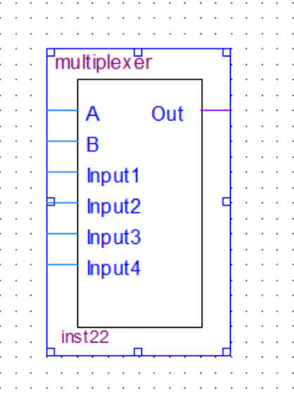
In this post, we’ll take a look at multiplexers and demultiplexers. In my 8-bit computer build, I only used multiplexers, you can see them being used in the clock generation circuits. I will however still cover demultiplexers in this post for the sake of completeness.
Multiplexers are used to select one of the multiple inputs and output it to one common output. Demultiplexers do the opposite of that and take in one input and put it out through one of the multiple outputs that was selected.
Let’s just take a look at the brief explanations and schematic bellow for a better understanding.
Multiplexer
The first part of the multiplexer is a decoder(see more about decoders in this post). It will take the binary input and decode it to one output. Then each one of the decoder outputs is feed into an AND gate together with one of the inputs. In the end, all the outputs of the AND gates get feed into an OR gate with multiple inputs.
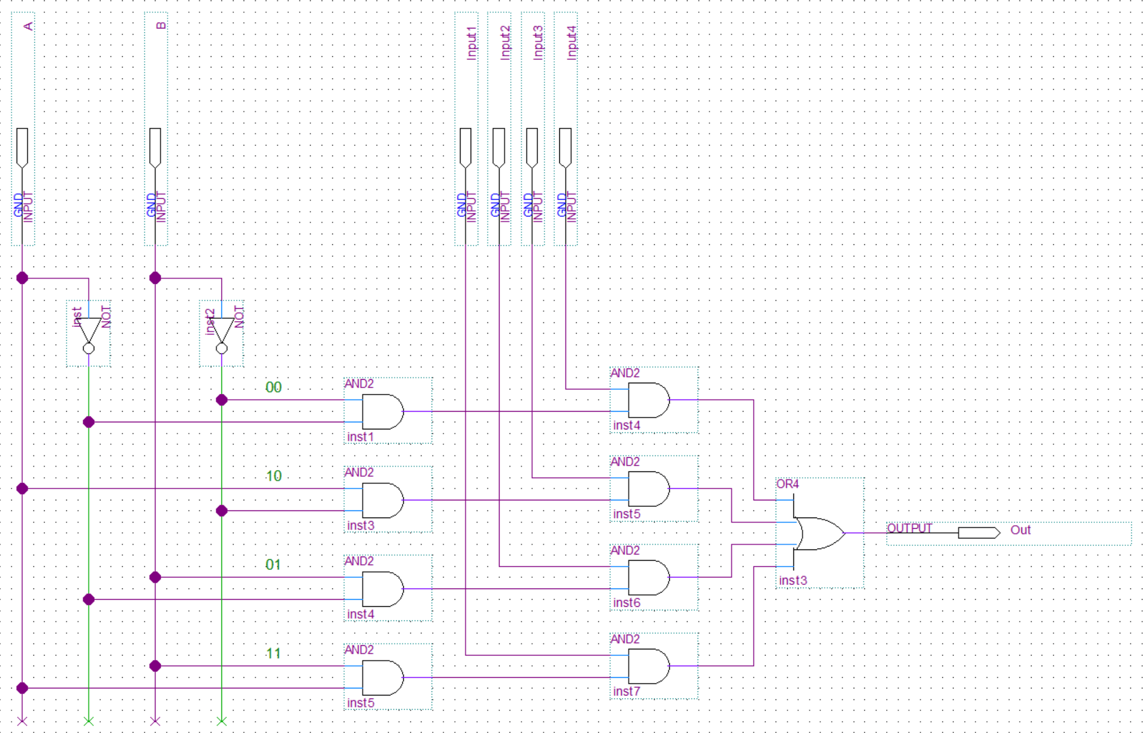
Truth Table
| A | B | Out |
|---|---|---|
| 0 | 0 | Input1 => Out |
| 1 | 0 | Input2 => Out |
| 0 | 1 | Input3 => Out |
| 1 | 1 | Input4 => Out |
Boolean Expression
Out = A'.B'.Input1 + A'.B.Input2 + A.B'.Input3 + A.B.Input4
Demultiplexer
The demultiplexer is basically just a decoder(see more about decoders in this post). It will take the binary input and decode it to one output. Compared to a regular decoder the demultiplexer also takes the data input line and conects to the input of every AND gate in the decoder.
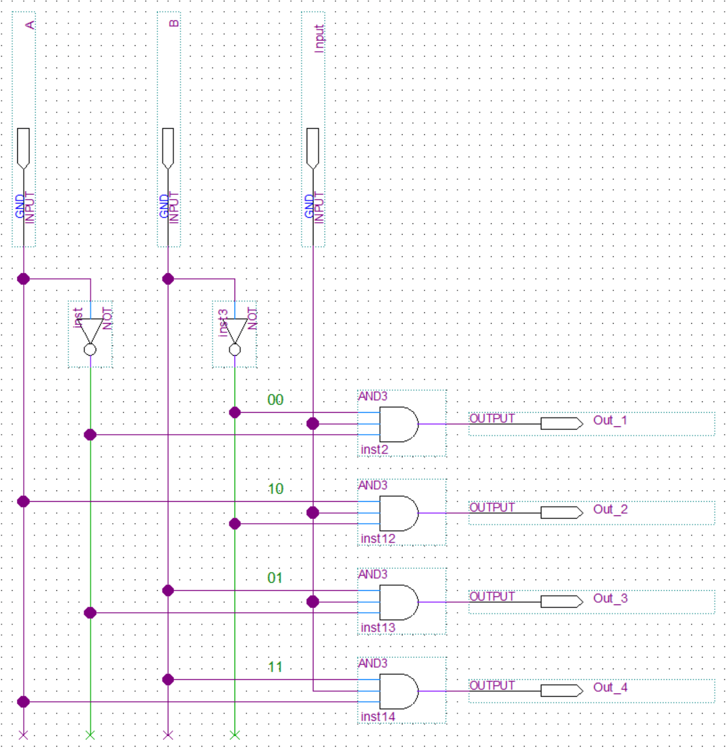
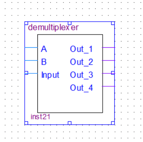
Truth Table
| A | B | Out |
|---|---|---|
| 0 | 0 | Input => Out_1 |
| 1 | 0 | Input => Out_2 |
| 0 | 1 | Input => Out_3 |
| 1 | 1 | Input => Out_4 |
Boolean Expression
Out_1 = A'.B'.Input
Out_2 = A.B'.Input
Out_3 = A'.B.Input
Out_4 = A.B.Input
Out_2 = A.B'.Input
Out_3 = A'.B.Input
Out_4 = A.B.Input
About
In this post, I will show how I made the registers for my 8-bit computer. I will use the flip-flops I made in this post.
And just like with the flip-flops you could use the premade register provided in Quartus. However, I wanted to build my own from scratch to truly understand how they work.
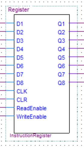
Register
The register is 8-bit as I made it for an 8-bit computer. This of course means it will have 8 inputs and outputs. Additionally, it will have a clear input to clear the register contents, a clock input, a read enable input to read in the data and a write enable input to output the register contents.
Internal Design Of The Register
I only included the last two memory cells in the picture as the design just repeats 6 more times(once for every bit). As you can see I am using a D edge-triggered flip-flop as a memory cell to store the data.
There are tristate buffers on the outputs to control the output. Tristate buffers are used instead of AND gates because the registers might be connected to a bus. Unlike AND gates which would pull the bus low the tristate buffers will be in a state of high impedance thus not interfering with the bus.
The clock inputs are all just connected together, the same goes for the clear inputs.
Last but most definitely not least are the memory refresh circuits(two AND and one OR gate before each flip-flop). On every rising edge of the clock, the flip-flop will read in the data from the inputs. Not quite what you would want for storing data(unless you happen to be reading data in at that moment). This is why we need the refresh circuit which just feeds the output of the flip-flop back to its input unless the read enable is high. In that case, it will connect the input of the register directly to the input of the flip-flop.

About
This post is about the Arduino programmer I made for the 8-Bit Computer in an FPGA. I will show how to use it, connect it, and briefly explain how it works. If you are interested in the source code you can get it all here on Github. This programmer should also be compatible with a normal breadboard computer like the one Ben Eater made in his video series.
Simple Version
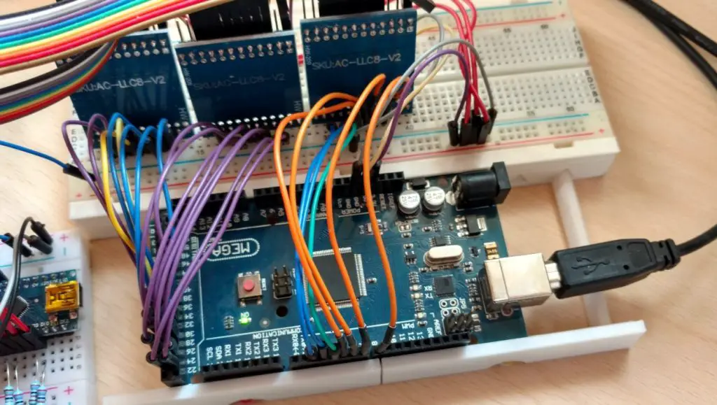
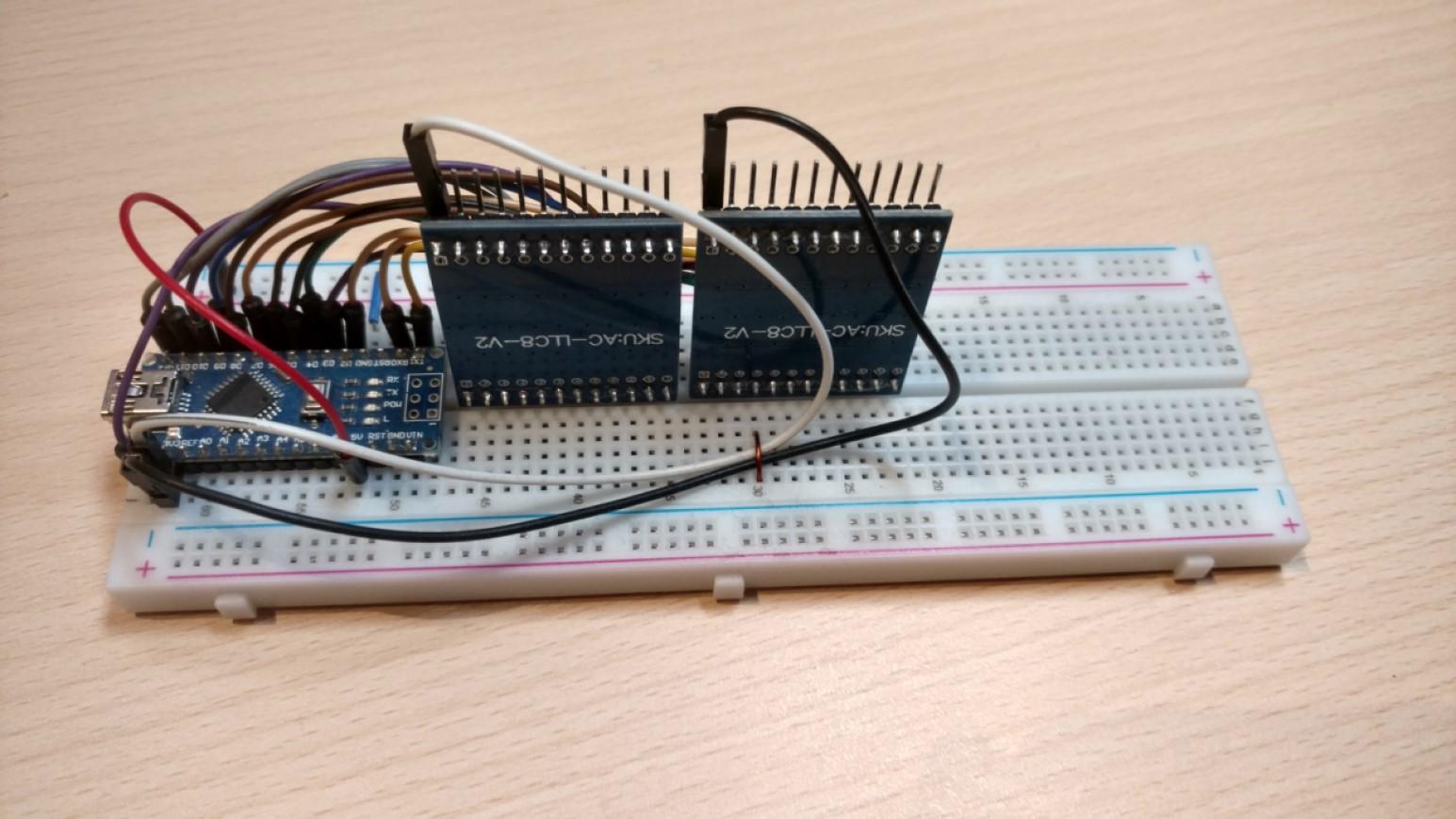
This is the first version of the programmer I made. It’s made from an Arduino nano. The limitation of this design is that you can only have a 4 bit memory address and 8 bit values(otherwise you run out of pins on the nano). The Arduino also has to be reprogrammed with every change to the machine code.
The two extra circuit boards are logic level converters. The FPGA I used has 3.3V IOs meanwhile the Arduino IO is 5V. If you built a breadboard computer with CMOS chips you can connect them straight up to the Arduino.
Connections to a breadboard computer:
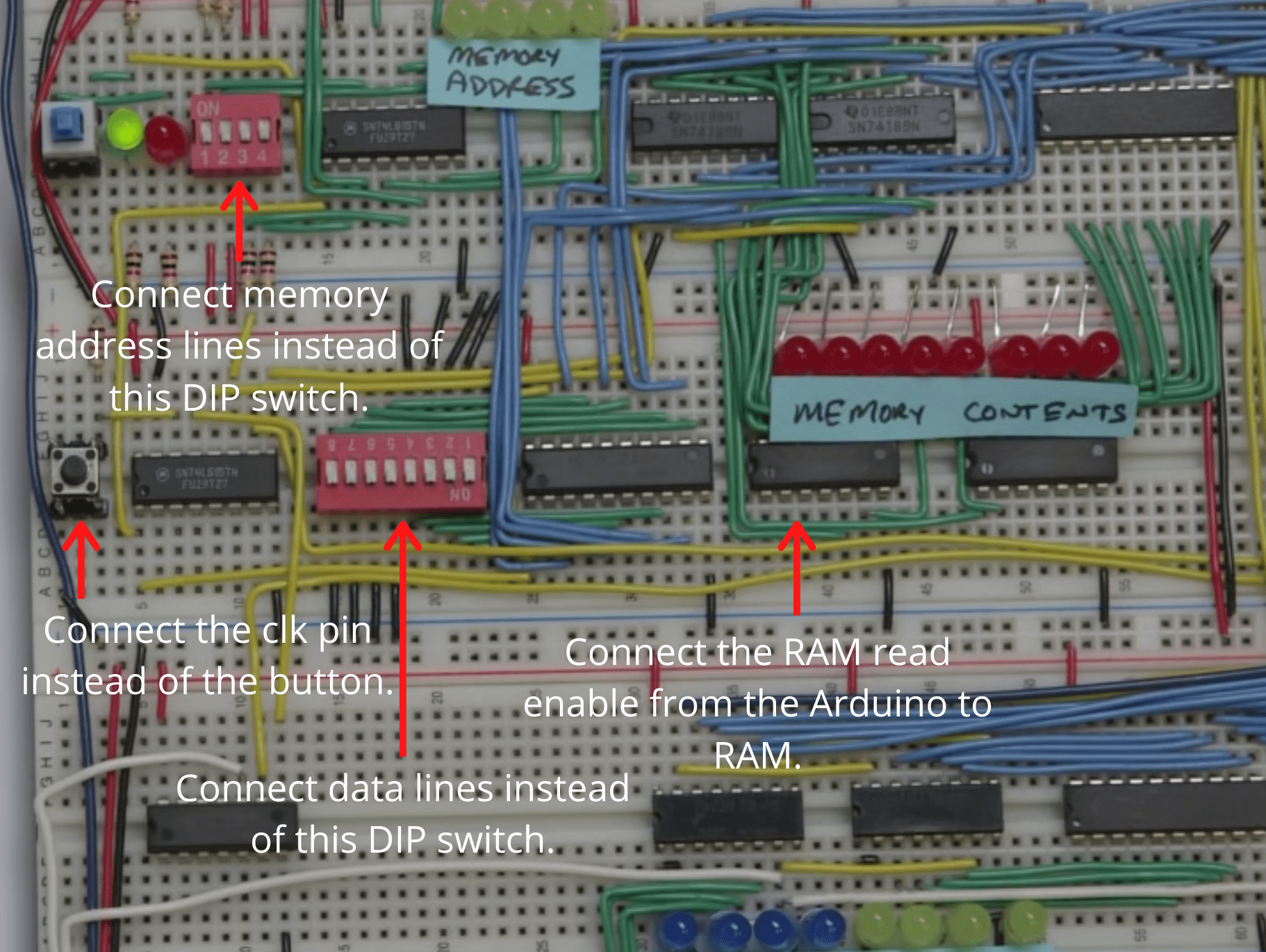
In the image below, you can see how you would connect the programmer to the 8-bit breadboard computer Ben Eater made.
Arduino code:
void setup() {
  //Set pins.
  pinMode(0, OUTPUT);
  pinMode(1, OUTPUT);
  pinMode(2, OUTPUT);
  pinMode(3, OUTPUT);
  pinMode(4, OUTPUT);
  pinMode(5, OUTPUT);
  pinMode(6, OUTPUT);
  pinMode(7, OUTPUT);
  pinMode(8, OUTPUT);
  pinMode(9, OUTPUT);
  pinMode(10, OUTPUT);
  pinMode(11, OUTPUT);
  pinMode(12, OUTPUT);
  pinMode(13, OUTPUT);

  //Array containing your machine code.
  int dataArray [16][12]{
        //LSB                 MSB     MEM. ADDR.
        { 1, 0, 0, 0,  0, 1, 1, 1,    0, 0, 0, 0},  //1
        { 0, 1, 0, 0,  1, 1, 1, 1,    1, 0, 0, 0},  //2
        { 1, 1, 0, 0,  0, 0, 0, 0,    0, 1, 0, 0},  //3
        { 0, 0, 1, 0,  0, 0, 0, 0,    1, 1, 0, 0},  //4
        { 0, 0, 0, 0,  0, 0, 0, 0,    0, 0, 1, 0},  //5
        { 0, 0, 0, 0,  0, 0, 0, 0,    1, 0, 1, 0},  //6
        { 0, 0, 0, 0,  0, 0, 0, 0,    0, 1, 1, 0},  //7
        { 0, 0, 0, 0,  0, 0, 0, 0,    1, 1, 1, 0},  //8
        { 0, 0, 0, 0,  0, 0, 0, 0,    0, 0, 0, 1},  //9
        { 0, 0, 0, 0,  0, 0, 0, 0,    1, 0, 0, 1},  //10
        { 0, 0, 0, 0,  0, 0, 0, 0,    0, 1, 0, 1},  //11
        { 0, 0, 0, 0,  0, 0, 0, 0,    1, 1, 0, 1},  //12
        { 0, 0, 0, 0,  0, 0, 0, 0,    0, 0, 1, 1},  //13
        { 0, 0, 0, 0,  0, 0, 0, 0,    1, 0, 1, 1},  //14
        { 0, 0, 1, 0,  0, 0, 0, 0,    0, 1, 1, 1},  //15
        { 0, 1, 0, 0,  0, 0, 0, 0,    1, 1, 1, 1},  //16
  };

  delay(1000);
  writeToRAM(dataArray);
  resetLines();
}

void loop() {

}

static void resetLines(){
  //Bus
  digitalWrite(0, LOW);
  digitalWrite(1, LOW);
  digitalWrite(2, LOW);
  digitalWrite(3, LOW);
  digitalWrite(4, LOW);
  digitalWrite(5, LOW);
  digitalWrite(6, LOW);
  digitalWrite(7, LOW);

  //RAM Adress
  digitalWrite(8, LOW);
  digitalWrite(9, LOW);
  digitalWrite(10, LOW);
  digitalWrite(11, LOW);

  //CLK
  digitalWrite(12, LOW);

  //RAM RE
  digitalWrite(13, LOW);
}

static void writeToRAM(int dataArray [16][12] ){
  //Iterate through the machine code array and toggle the appropriate pins.
  for(int i = 0; i < 16; i++){
      //Bus
      digitalWrite(0, getState(dataArray[i][0]));
      digitalWrite(1, getState(dataArray[i][1]));
      digitalWrite(2, getState(dataArray[i][2]));
      digitalWrite(3, getState(dataArray[i][3]));
      digitalWrite(4, getState(dataArray[i][4]));
      digitalWrite(5, getState(dataArray[i][5]));
      digitalWrite(6, getState(dataArray[i][6]));
      digitalWrite(7, getState(dataArray[i][7]));

      //RAM Adress
      digitalWrite(8, getState(dataArray[i][8]));
      digitalWrite(9, getState(dataArray[i][9]));
      digitalWrite(10, getState(dataArray[i][10]));
      digitalWrite(11, getState(dataArray[i][11]));


      //RAM RE
      digitalWrite(13, HIGH);
      delay(10);

      //Delay clock so the data can get to the destination before the rising edge of the clock.
      //delay(100);

      //CLK
      digitalWrite(12, HIGH);
      delay(100);
      digitalWrite(12, LOW);
      delay(10);

      //RAM RE
      digitalWrite(13, LOW);

      //Delay before next program cycle.
      delay(100);
  }
}

static bool getState(int bitValue){
    if(bitValue == 0){
      return false;
    }else{
      return true;
    }
}
From the Arduino sketch you can see that pins 0-7 are data lines, 8-11 are memory address lines, 12 is RAM read enable and 13 is the clock.
To program you computer you first need to write your program in machine code. Then you enter your machine code into the dataArray. The first 8 numbers are the memory content while the last 4 are the memory address. After you do that you have to flash the sketch to the Arduino.
Finally, you can just use the reset button on the Arduino to initiate the programming process as when the Arduino resets the program will execute.
After the computer has been programmed the Arduino programmer has to be disconnected or turned off as otherwise it will pull down the data lines. This can also be avoided if you connect the Arduino to your RAM through OR gates(this is what I did with my computer).
Programmer with an "IDE"
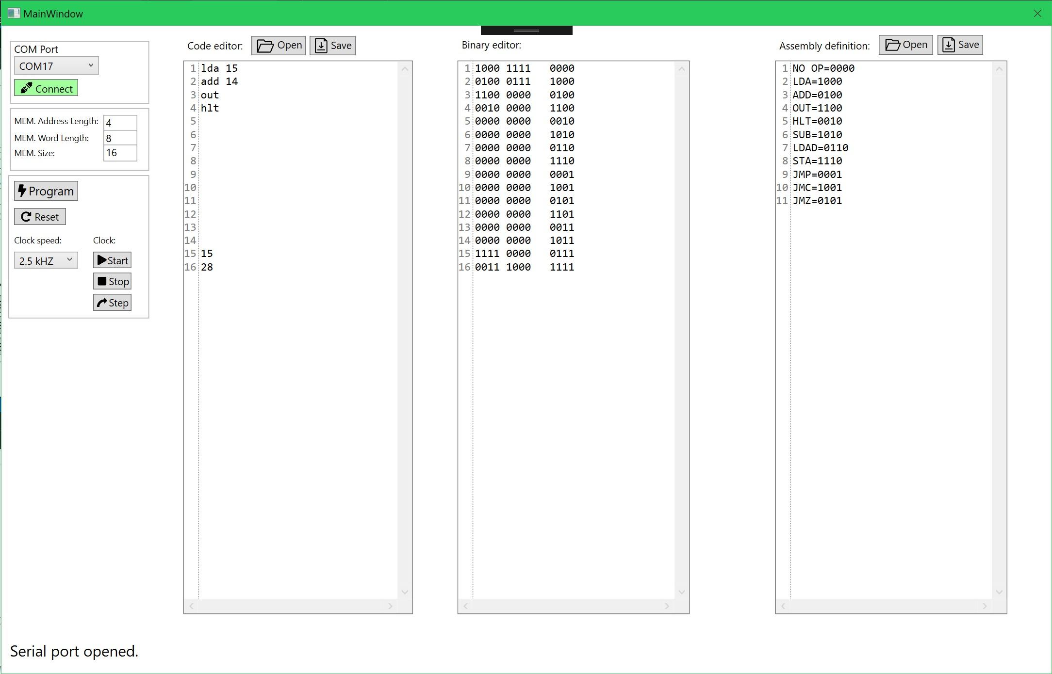
To make programming the 8-bit computer even easier I decided to make a simple sort of an IDE that can connect to the Arduino programmer and program the computer through it without having to reflash it with every change of the program.
The IDE has three code editors. The last window has the assembly definition where you map your custom machine code for the specific computer you made to your specific custom assembly language you made. Then you can write an assembly program in the first code editor. The machine code will automatically get generated in the middle editor.
On the left, you have the controls column. At the very top, you can establish a COM port connection to the Arduino.
Then you have the option to set your RAM size, RAM word length, and the memory address length. Currently, this is fixed and can’t be changed. I didn’t really need the option for a bigger memory so I skipped implementing this feature(might add it in the future).
I won’t post the code for the IDE here as it’s too long. You can see and download the whole project from Github. For the explanation of the code read the comments.
I used an Arduino Mega because it has more IO pins than the nano. This enables future expansions for RAM size and it enables the use of control signals to start/stop/reset the computer from the IDE.
The hardware connections to the breadboard computer would be almost the same as they were in the image above with the simple version of the programmer. The exception would be that you would have to connect the control signals to your clock start/stop/step buttons, reset button. For setting the clock speed using the programmer you would however have to slightly redesign your clock module.
Arduino Code:
const byte numChars = 27;
char receivedChars[numChars];
int memData[16][12];
byte memCounter = 0;
boolean newData = false;
boolean dataStart = false;

//Pin assignments///////////////
const byte strtClkPin = 36;
const byte stopClkPin = 37;
const byte rsetPin = 2;
const byte progEnPin = 3;
const byte clkStpPin = 4;
const byte clkSetPin1 = 5;
const byte clkSetPin2 = 6;
const byte clkSetPin3 = 7;
const byte clkSetPin4 = 8;
////////////////////////////////

void setup() {
  setPinModes();
  Serial.begin(115200);

  digitalWrite(progEnPin, LOW);
  stopClock();
  resetDevice();
  digitalWrite(clkSetPin1, LOW);
  digitalWrite(clkSetPin2, LOW);
  digitalWrite(clkSetPin3, LOW);
  digitalWrite(clkSetPin4, LOW);
}

void loop() {
    rxData();
    rxMemDataEnd();
}

void rxData() {
    static byte count = 0;
    char ch;

  //Check if serial data is available.
    while(Serial.available() > 0 && newData == false) {
        //Read and remove character from the serial buffer.
        ch = Serial.read();

        //Check if it's the start of the data.
        if(ch == '_'){
          dataStart = true;
        }

        if(dataStart && ch != '_'){
          if(ch != '\n'){
              receivedChars[count] = ch;
              count++;
              if(count >= numChars){
                  count = numChars - 1;
              }
          }
          else{
              //Terminate string.
              receivedChars[count] = '\0';

              char command[5];

              getCommand(command);

              if(strcmp(command, "prog") == 0){
                getMemData();
              }else if(strcmp(command, "strt") == 0){
                startClock();
                Serial.print("strt done");
              }else if(strcmp(command, "stop") == 0){
                stopClock();
                Serial.print("stop done");
              }else if(strcmp(command, "step") == 0){
                clockStep();
                Serial.print("step done");
              }else if(strcmp(command, "rset") == 0){
                resetDevice();
                Serial.print("rset done");
              }else if(strcmp(command, "clks") == 0){
                setClockSpeed();
                Serial.print("clks done");
              }else if(strcmp(command, "prst") == 0){
                programmerReset();
                Serial.print("prst done");
              }else{
                Serial.print("Bad command!");
              }

              count = 0;
              newData = true;
              dataStart = false;
            }
       }
    }
}

static void programmerReset(){
  //Reset variables.
  memCounter = 0;
  newData = false;
  dataStart = false;

  //Empty serial buffer.
  while(Serial.available() > 0){
    Serial.read();
  }
}

//Currently not used.
static void getInfo(int *memInfo){
  char memAddressLengthStr[3];
  char memLocationLengthStr[3];
  char memLocationCountStr[6];

  for(int i = 4; i <= 12; i++){
    if(i <= 5){
      memAddressLengthStr[i-4] = receivedChars[i];
      if(i-4 == 1){
        memAddressLengthStr[i-3] = '\0';
      }
    }else if(i <= 7){
      memLocationLengthStr[i-6] =  receivedChars[i];
      if(i-6 == 1){
        memLocationLengthStr[i-5] = '\0';
      }
    }else if(i <= 12){
      memLocationCountStr[i-8] =  receivedChars[i];

      if(i-11 == 1){
        memLocationCountStr[i-7] = '\0';
      }
    }
  }

  //Convert char to
  memInfo[0] = atoi(memAddressLengthStr);
  memInfo[1] = atoi(memLocationLengthStr);
  memInfo[2] = atoi(memLocationCountStr);

}

static void getClockSpeed(int *clkSpeedValues){
  for(int i = 4; i <= 7; i++){
    clkSpeedValues[i-4] = (receivedChars[i] - '0');
  }
}

static void setClockSpeed(){
  int clkSpeedValues[4];

  getClockSpeed(clkSpeedValues);

  digitalWrite(clkSetPin1, getState(clkSpeedValues[0]));
  digitalWrite(clkSetPin2, getState(clkSpeedValues[1]));
  digitalWrite(clkSetPin3, getState(clkSpeedValues[2]));
  digitalWrite(clkSetPin4, getState(clkSpeedValues[3]));
}

static void setPinModes(){
  //Data pins///////////////
  pinMode(22, OUTPUT); //LSB
  pinMode(23, OUTPUT);
  pinMode(24, OUTPUT);
  pinMode(25, OUTPUT);

  pinMode(26, OUTPUT);
  pinMode(27, OUTPUT);
  pinMode(28, OUTPUT);
  pinMode(29, OUTPUT); //MSB
  //////////////////////////

  //Mem. Add. Pins/////////
  pinMode(30, OUTPUT);
  pinMode(31, OUTPUT);
  pinMode(32, OUTPUT);
  pinMode(33, OUTPUT);
  /////////////////////////

  //Clk
  pinMode(34, OUTPUT);
  //RAM read enable
  pinMode(35, OUTPUT);

  //Start
  pinMode(strtClkPin, OUTPUT);
  //Stop
  pinMode(stopClkPin, OUTPUT);

  //Clear
  pinMode(rsetPin, OUTPUT);
  //Program enable
  pinMode(progEnPin, OUTPUT);
  //Step
  pinMode(clkStpPin, OUTPUT);

  //Clk speed selection//
  pinMode(clkSetPin1, OUTPUT);
  pinMode(clkSetPin2, OUTPUT);
  pinMode(clkSetPin3, OUTPUT);
  pinMode(clkSetPin4, OUTPUT);
  ///////////////////////
}

static void getMemData(){
  for(int i = 0; i <= 11 ; i++){
    memData[memCounter][i] = (receivedChars[i+13] - '0');
  }

  //Next mem. position.
  memCounter++;
}

static void getCommand(char *command){
  for(int i = 0; i <= 3; i++){
    command[i] = receivedChars[i];
  }

  //Terminate string.
  command[4] = '\0';
}

static void rxMemDataEnd(){
    //If new data is available.
    if(newData == true){
      //Check if data transfer is over.
      if(memCounter == 16){
        writeToRAM();

        //Reset.
        memCounter = 0;

        Serial.print("prog done");
      }else{
        //Signal that the data was read.
        Serial.print("ok");
      }

      //Reset.
      newData = false;
      delay(10);
    }
}

static void clockStep(){
  digitalWrite(clkStpPin, HIGH);
  delay(50);
  digitalWrite(clkStpPin, LOW);
}

static void resetDevice(){
  digitalWrite(rsetPin, HIGH);
  delay(50);
  digitalWrite(rsetPin, LOW);
}

static void startClock(){
  digitalWrite(strtClkPin, HIGH);
  delay(50);
  digitalWrite(strtClkPin, LOW);
}

static void stopClock(){
  digitalWrite(stopClkPin, HIGH);
  delay(50);
  digitalWrite(stopClkPin, LOW);
}

static void writeToRAM(){
  stopClock();
  resetDevice();
  digitalWrite(progEnPin, HIGH);
  delay(10);

  //Iterate through the machine code array and toggle the appropriate pins.
  for(int i = 0; i < 16; i++){
      //Bus
      digitalWrite(22, getState(memData[i][0]));
      digitalWrite(23, getState(memData[i][1]));
      digitalWrite(24, getState(memData[i][2]));
      digitalWrite(25, getState(memData[i][3]));
      digitalWrite(26, getState(memData[i][4]));
      digitalWrite(27, getState(memData[i][5]));
      digitalWrite(28, getState(memData[i][6]));
      digitalWrite(29, getState(memData[i][7]));

      //RAM Adress
      digitalWrite(30, getState(memData[i][8]));
      digitalWrite(31, getState(memData[i][9]));
      digitalWrite(32, getState(memData[i][10]));
      digitalWrite(33, getState(memData[i][11]));


      //RAM RE
      digitalWrite(35, HIGH);
      delay(10);

      //Delay clock so the data can get to the destination before the rising edge of the clock.
      //delay(100);

      //CLK
      digitalWrite(34, HIGH);
      delay(10);
      digitalWrite(34, LOW);
      delay(10);

      //RAM RE
      digitalWrite(35, LOW);

      //Delay before next program cycle.
      delay(10);
  }

  //PROG EN
  digitalWrite(progEnPin, LOW);
}

static bool getState(int bitValue){
    if(bitValue == 0){
      return false;
    }else if(bitValue == 1){
      return true;
    }
}
Here I will briefly describe how the code works(for more detail see the code and the comments).
The Arduino receives the values over the serial port from the App. First, it determines what command it has just received. After that, it will execute the appropriate action like start, stop, program, … The machine code data arrives to the Arduino in chunks(each mem. address is one chunk) and is then stored in an array. This keeps happening until the last chunk of data has been received. Finally, the processes to shift all the values from the array into the 8-bit computers RAM begins. This is done by toggling the IO pins high/low depending on the values in the array.
I know that storing the values in the Arduino isn’t the best solution. Ideally, the data should just be immediately written into the computers RAM without being buffer in an array. The reason things work the way they do is that I just upgraded the code from the simple version of the programmer. So if there is a need for it I might update the programmer and IDE in the future.
Programming Demonstration
About
In this post, we’ll take a look at the flip-flop which is one of the most common and essential logic blocks used in digital logic design. It can be used used for lots of different things. If you take a look at my 8-bit computer build you will see that flip-flops are used all over the place.
You can use premade flip-flops provided in Quartus. However, I wanted to build my own from scratch to truly understand how they work.
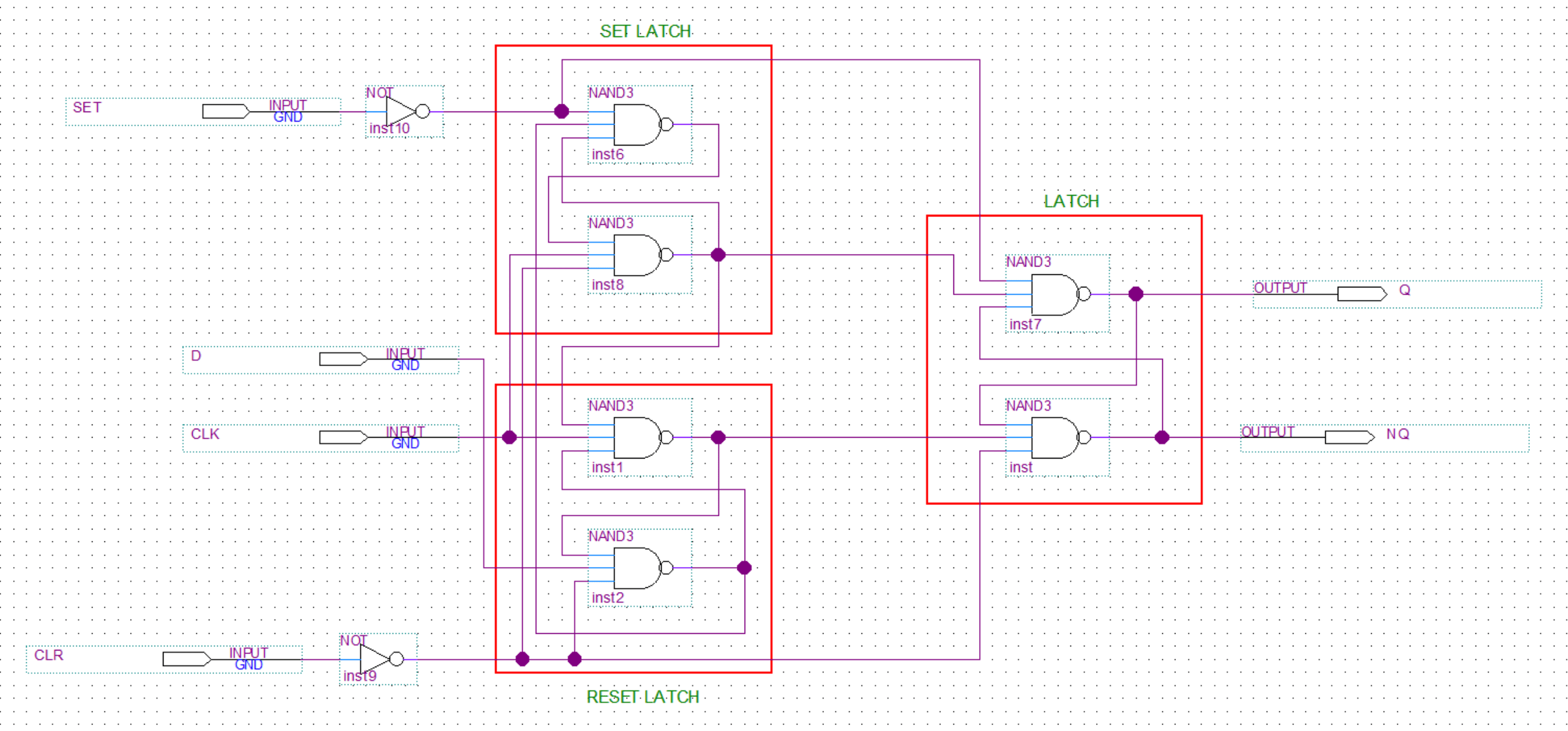
NAND Gate SR Latch
But before building a flip-flop let’s look at the most essential element required to make one: the SR latch.
SR latches are most commonly made from NAND or NOR gates. It doesn’t really matter what you use but I will stick with using NAND gates.
NAND Gate
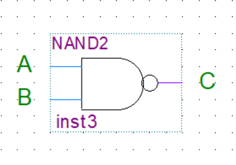
NAND Gate Truth Table
| A | B | C |
|---|---|---|
| 0 | 0 | 1 |
| 0 | 1 | 1 |
| 1 | 0 | 1 |
| 1 | 1 | 0 |
Now assuming you know the behavior/truth table of NAND gates we can explore how they can form a latching circuit that can store state. This is achieved by connecting the outputs of each gate one of the inputs of the other gate.
SR Latch
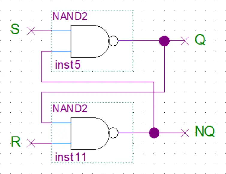
SR Latch Truth Table
| S | R | Q | NQ |
|---|---|---|---|
| 0 | 0 | / | / |
| 0 | 1 | 0 | 1 |
| 1 | 0 | 1 | 0 |
| 1 | 1 | 0 | 0 |
The S(set) input can be toggled to set Q to high or the R(reset) can be toggled to set Q low.
Below you can play around with the circuit yourself to see how it works. I think that this will be way more intuitive and easy to understand compared to me describing it with words.
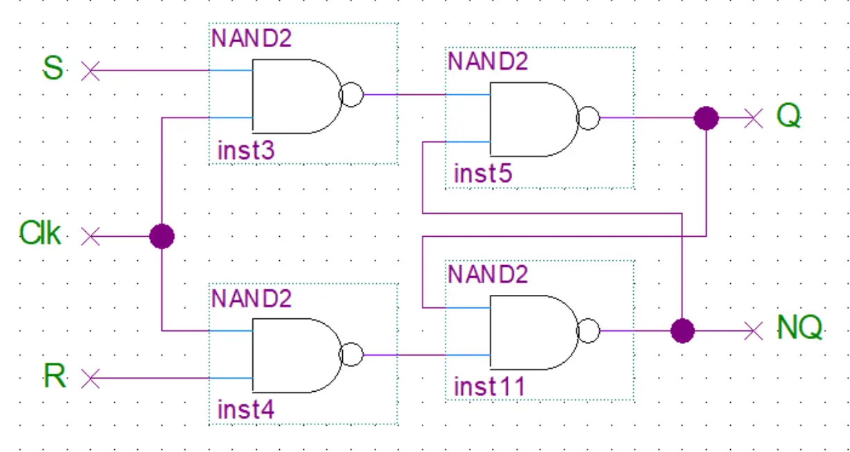
Clocked SR Flip Flop
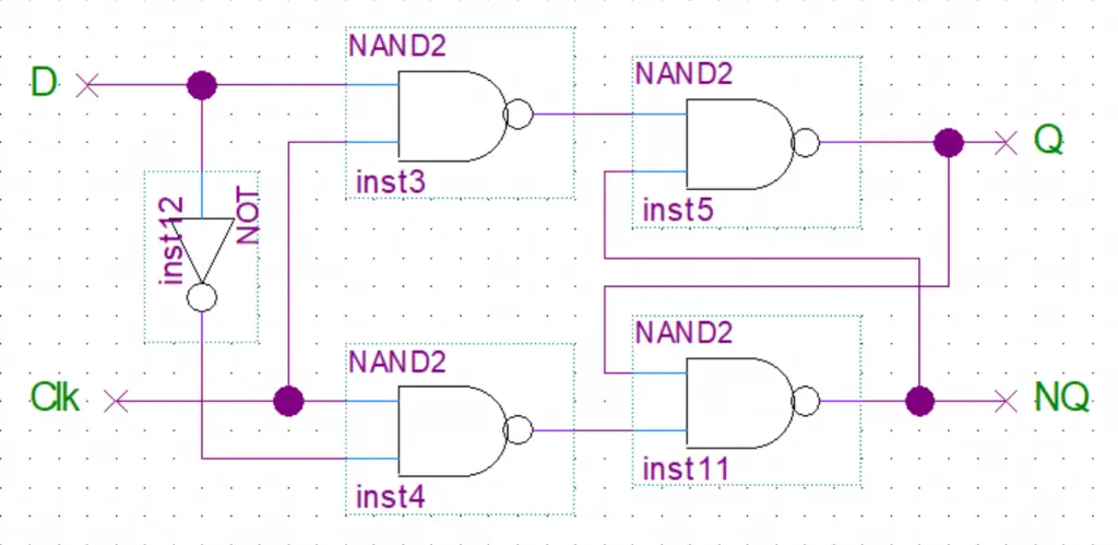
The SR latch will change state whenever the inputs change. But we want the state to change only on a certain condition like when the clock signal is present. To accomplish this we add a NAND gate to the S and R inputs. Then we tie together the inputs of those gates and use that as an input for the clock signal. While the other two outputs now become the S and R. Now the set/reset will only be possible while the clock signal is present.
D Flip Flop
The SR flip-flop still has two inputs(S,R) that require to be toggled separately to change the latched value from 0 to 1 or vice versa. We wouldn’t be able to store the value from a single dateline this way. What we want is a single input to which we can connect our data line. Then when the clock signal is present the value from the data line(0 or 1) gets stored in the latch.
This can simply be done by connecting the S input to the R input through a NOT gate.
Master Slave D Flip Flop
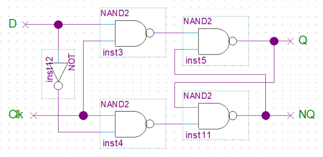
After making our D flip-flop we now stumble upon another problem. We only want the data to be read into our flip flop on the rising edge of the clock. If the signal changes after the rising edge of the clock we don’t want the change to be registered. To do that we can attach two D flip-flops one after another in a master-slave configuration(see below).
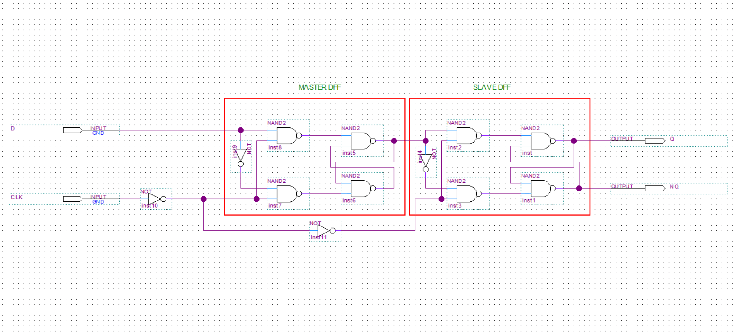
Edge Triggered D Flip Flop with Asynchronous Set and Reset
Ok, almost done now. The last thing we need to add is an asynchronous set/reset. This will be useful when resetting our computer as we can simply apply a 1 to the reset/clear input and the flip-flop Q output will reset to 0 without having to wait for the clock hence why it’s called asynchronous.
The design is a bit different here, you can see three latches. One to latch the set signal, one to latch the reset signal, and the final latch that stores the state. The NAND gates used here have three inputs so we can feed in the additional set/reset signal.
Here is a simulation of the final circuit for better understanding(but without the set and reset functionality).
Conclusion
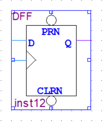
This is how I made the flip-flops I used in my 8-bit computer build. The simpler alternative would be to use the premade D flip-flop provided by Quartus and save yourself some time. 🙂 But hopefully, now you at least somewhat understand the inner workings of a flip-flop.
About
This project of mine was inspired by Ben Eater and the 8-Bit breadboard computer he made. I would in fact highly recommend you check out his complete video series on it. When I first saw his computer featured on Hackaday I thought it was awesome and immediately wanted to build my own.
But as I started to look into the components needed for the build I figured that it was kind of expensive. And building the computer on breadboards with logic chips would take up a lot of space, bring up problems with bad connections, etc … So instead I thought I could just make the computer in an FPGA(plus I wanted to get into FPGAs anyway). This way I could learn some stuff about working with FPGAs while making the 8-bit computer.
Well … as it turns out the FPGA dev board wasn’t that cheap either and debugging the FPGA designs can be kind of a pain as you don’t have easy access to the connections. So using an FPGA definitely has its drawbacks. Like … not having a cool looking breadboard computer at the end. For this reasson I might actually build an actual breadboard computer at some point in the future. But nonetheless, this whole thing was a great learning experience.
Despite using an FPGA I purposefully didn’t use HDL but made the computer by using discrete logic gates. I also mostly didn’t use any of the premade components in Quartus(FPGA development environment). If I had used HDL or the prebuilt components(flip flops, muxers, …) it would have been easier but I wouldn’t get to understand how a computer works at the logic gate level. This way it was way clearer to me how a computer is built and how it operates.
Project Files
All the project files are available in this GitHub repository.
Hardware used
- #adAmazon LinkDE0 Nano – Altera Cyclone IV FPGA development board
- #adAmazon LinkArduino Mega
- #adAmazon LinkArduino Nano x2
- #adAmazon LinkSSD1306 OLED Screen x2
- #adAmazon LinkLogic Level Converters
- #adAmazon LinkBreadboards
- #adAmazon LinkButtons
- #adAmazon LinkLEDs
- #adAmazon LinkResistors
- #adAmazon LinkWires
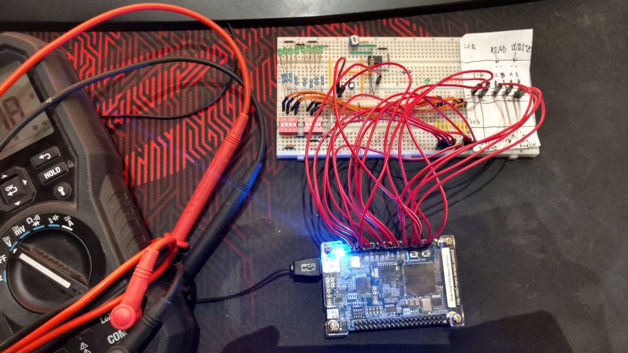
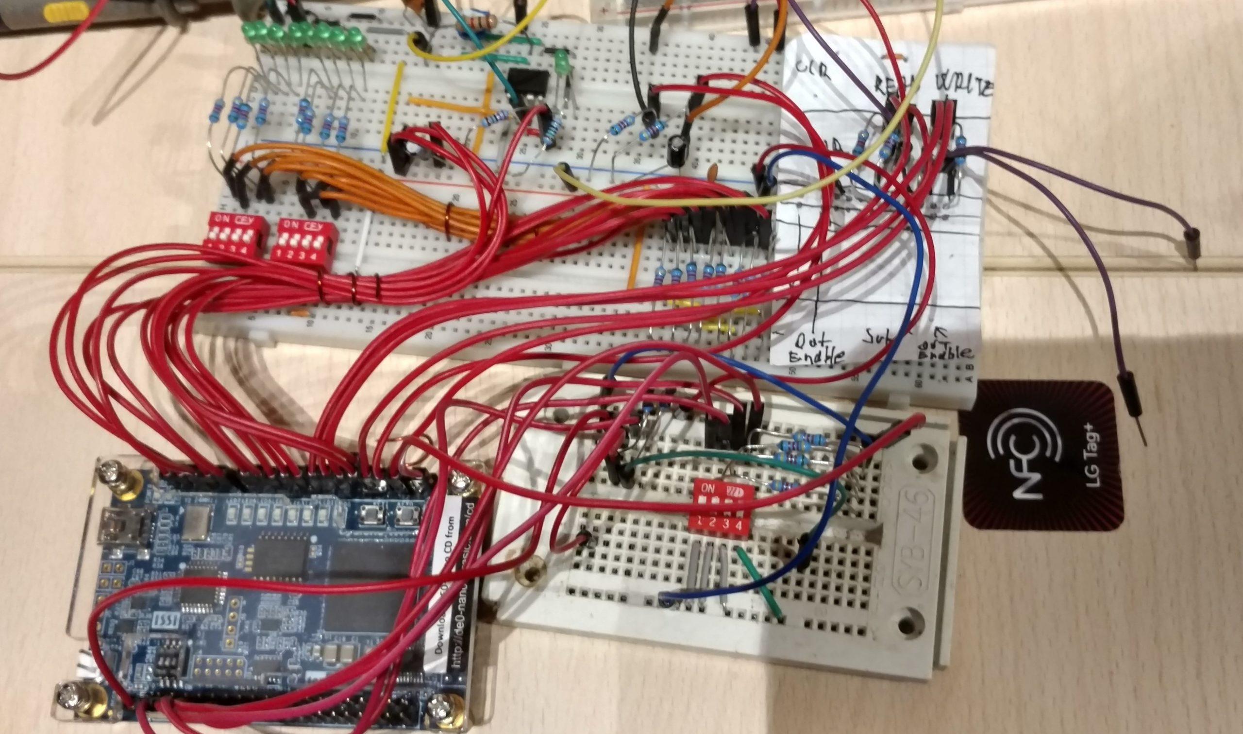
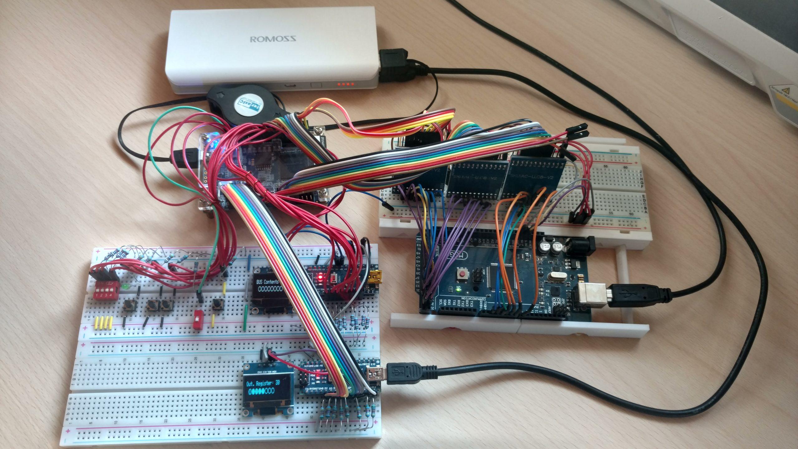
Hardware Connections
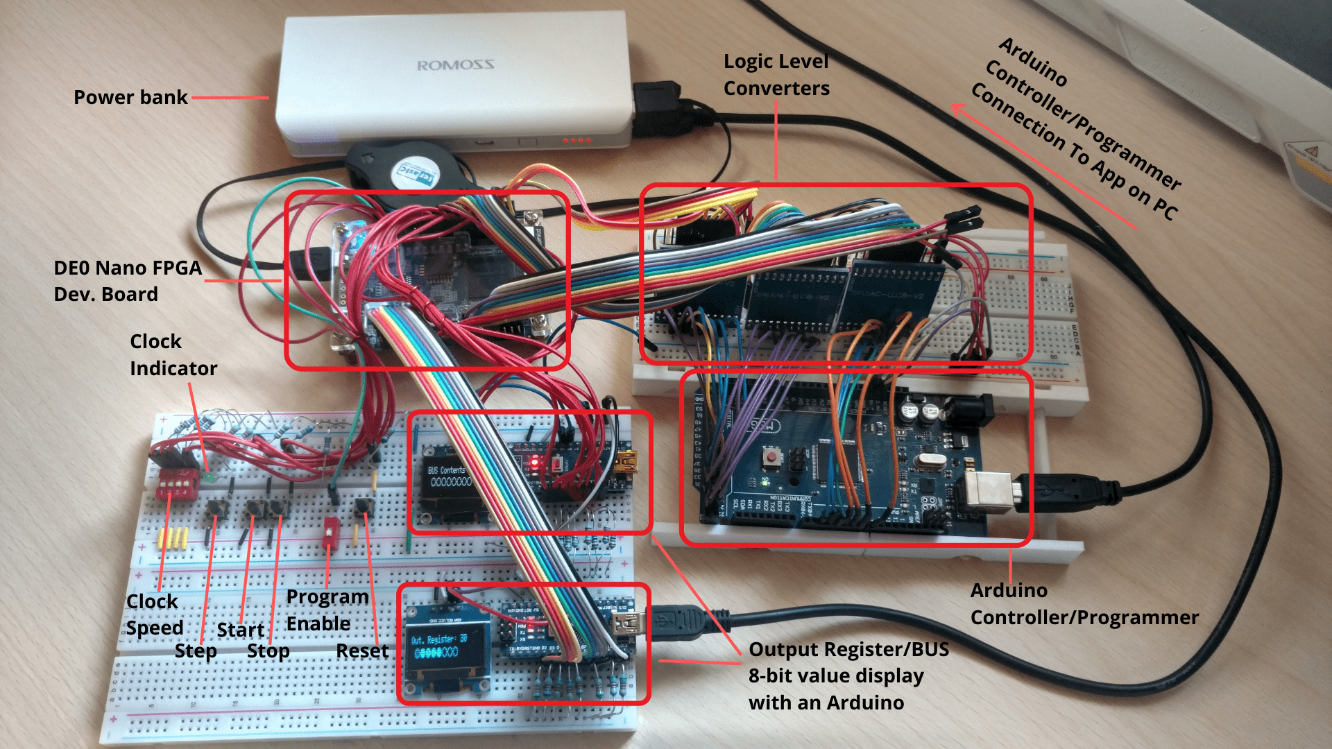
Description of the components in the image above:
- The FPGA development board contains the computer itself and it gets powered from the power bank above it.
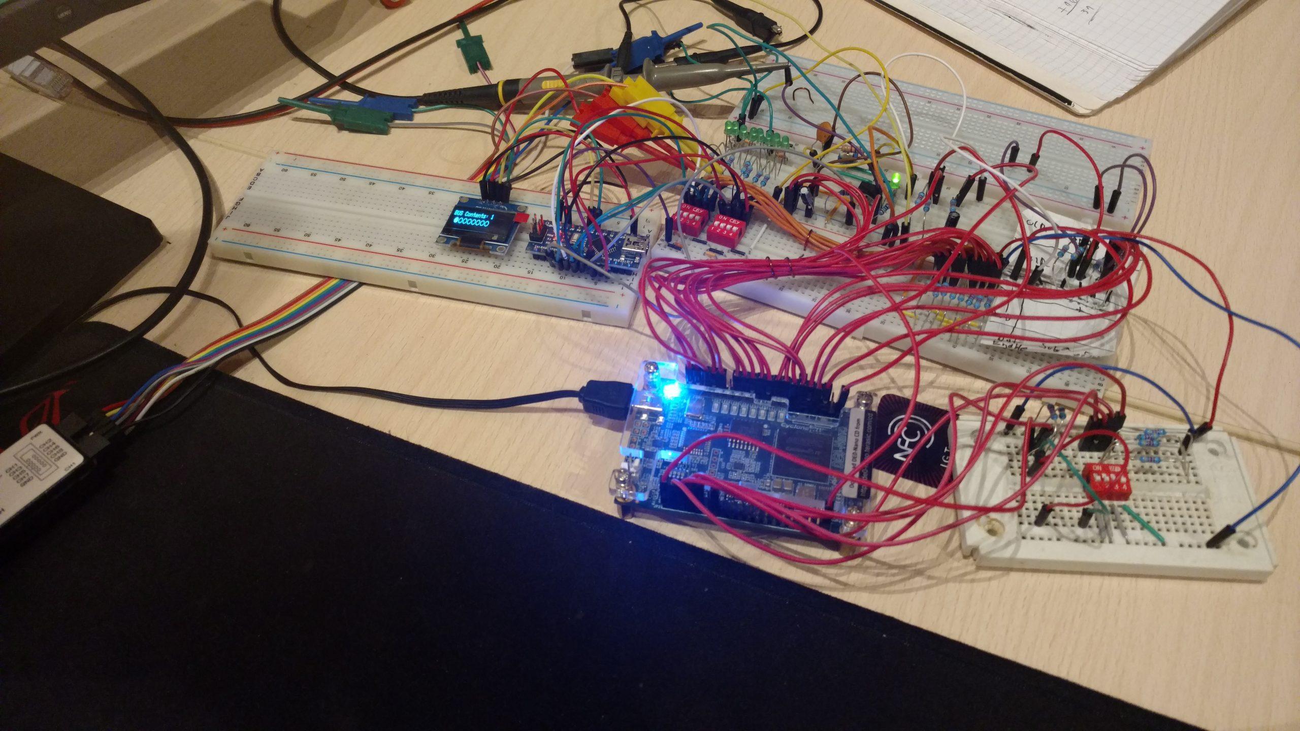
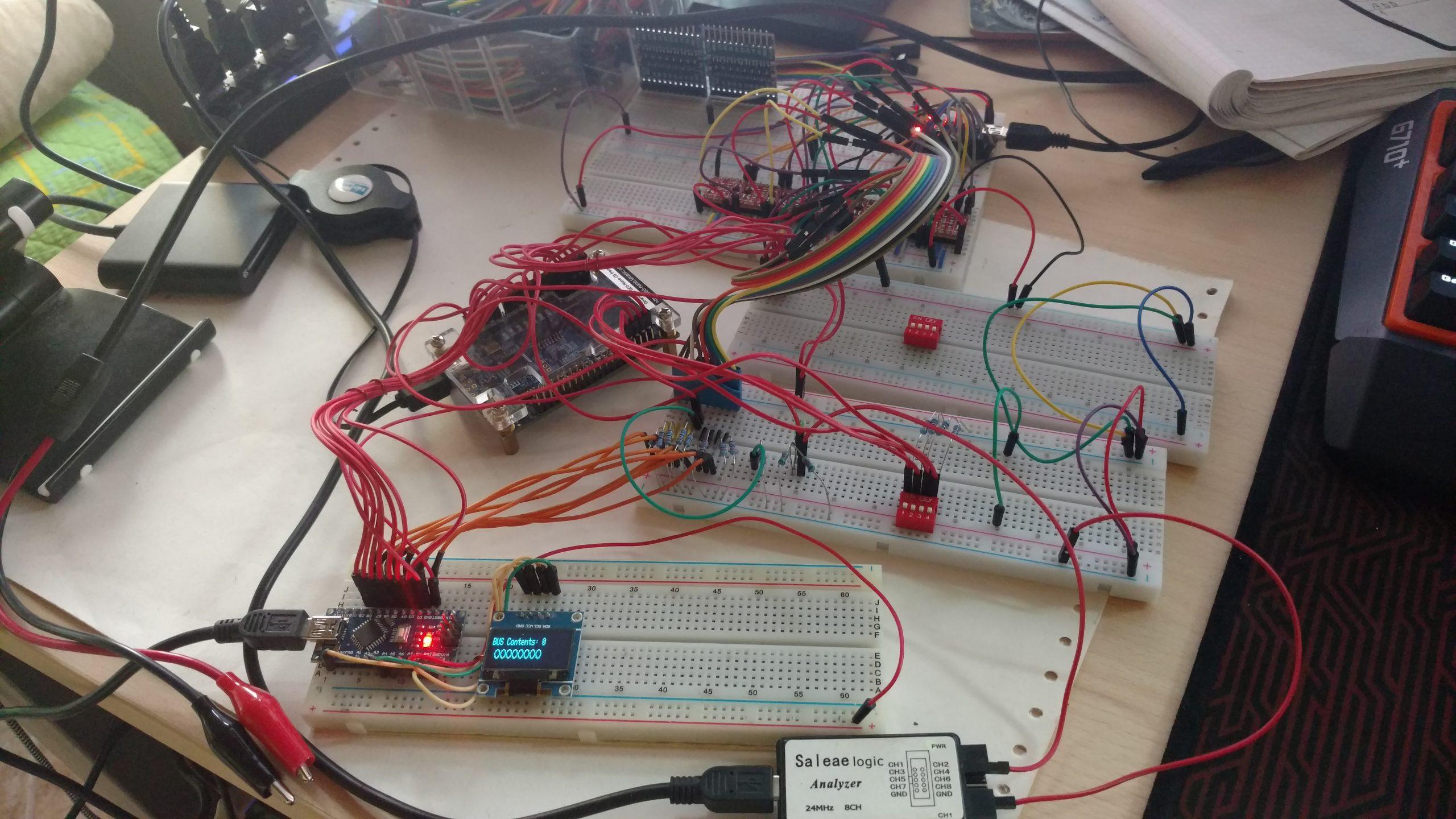
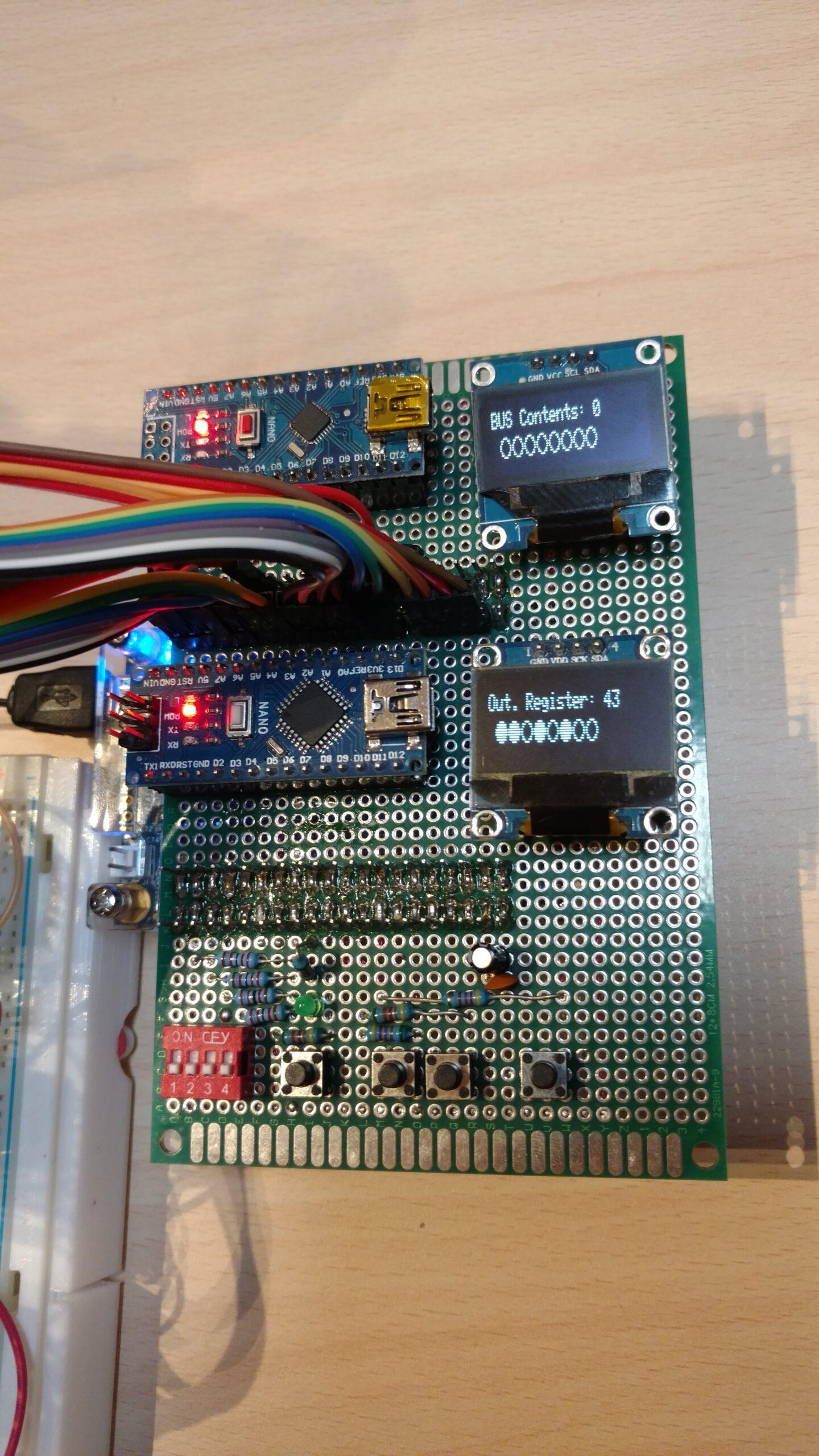
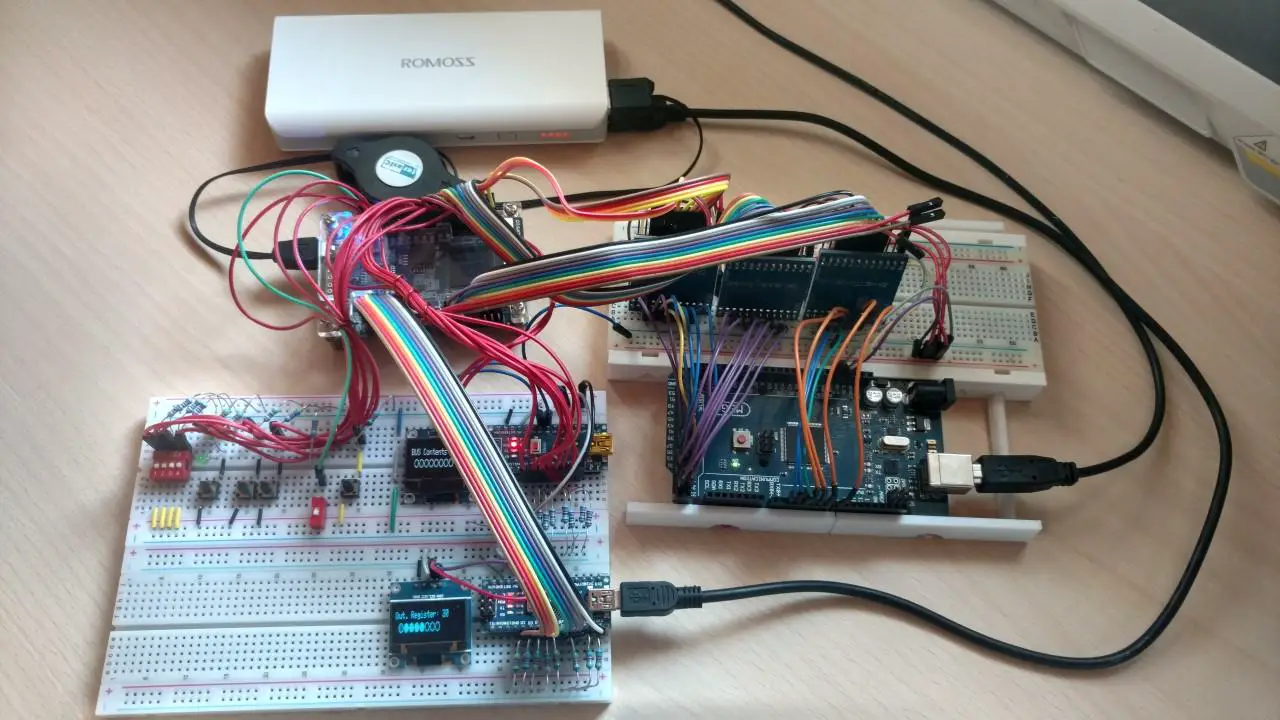
- The two Arduino minis just take the binary logic levels from the wires and display the value in decimal on an I2C SSD1306 OLED screen. They replace the LEDs and at the same time conveniently display the decimal value. You can still see the individual binary value represented by the circle at the bottom. I did this instead of using LEDs and/or a 7-segment display because it is more compact and it was easier and more convenient for me to make. Also, the Arduinos are powered separately(from the power bank) and thus don’t draw any current from the FPGA, unlike LEDs. I could’ve used some transistors to drive the LEDs but I think that would’ve looked kind of messy. The upper display shows the contents of the main bus while the bottom display shows the contents of the output register.
- On the breadboard, you can see all of the controls for the computer. Program Enable is not used with the current Arduino programmer. The DIP switch is used to select one of the 16 clock speeds.
- The logic level converters are used to convert the 5V signals from the Arduino to the 3.3V signals required for the FPGA.
- The Arduino Mega is used as a controller and a programmer. The computer can either be controlled by the buttons on the breadboard or from the application on the PC via the Arduino. The “software” or assembly can be written in the application on the PC and then loaded into the computer via the Arduino. The Arduino is connected to the 8-bit computers RAM and can load data straight into it.
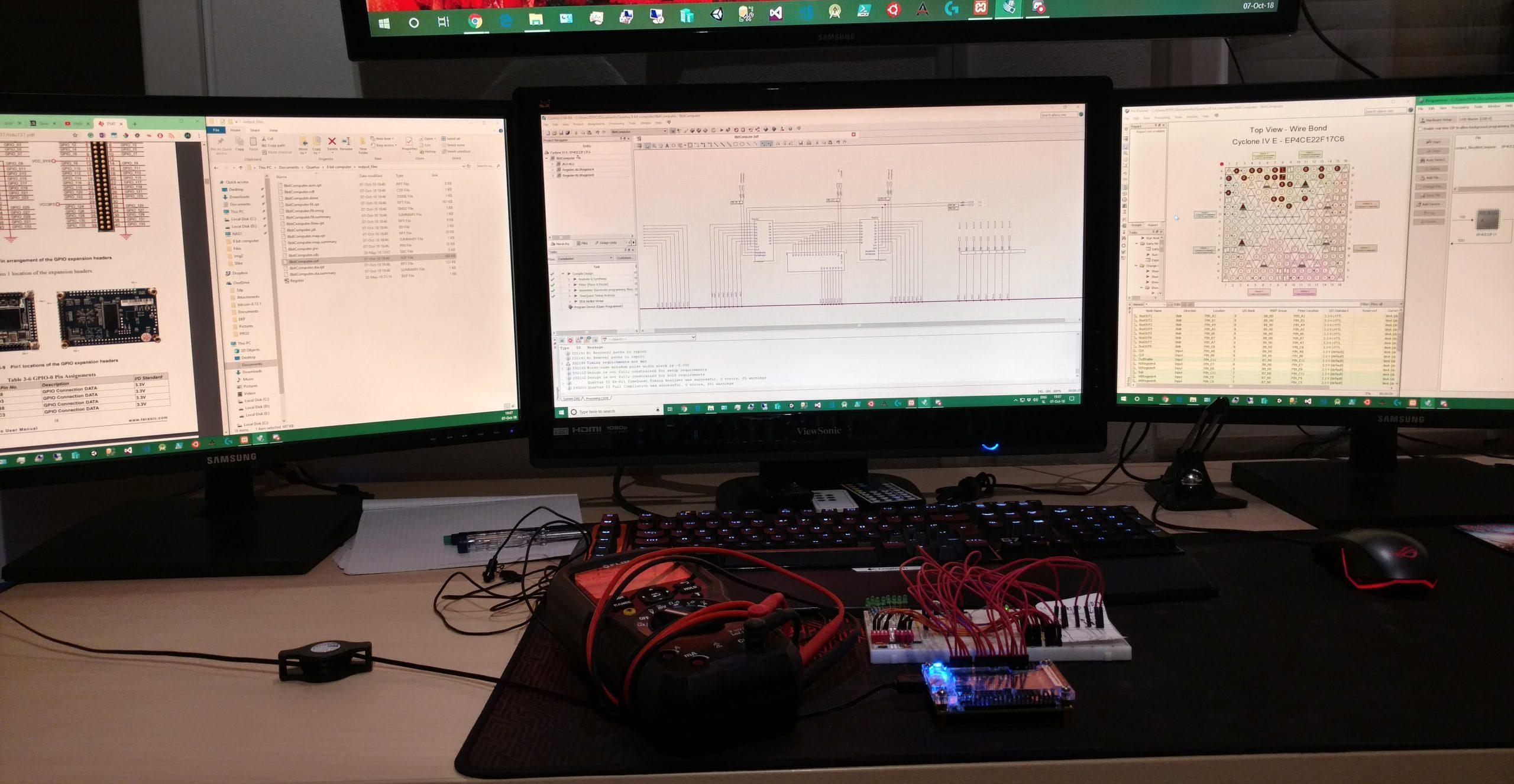
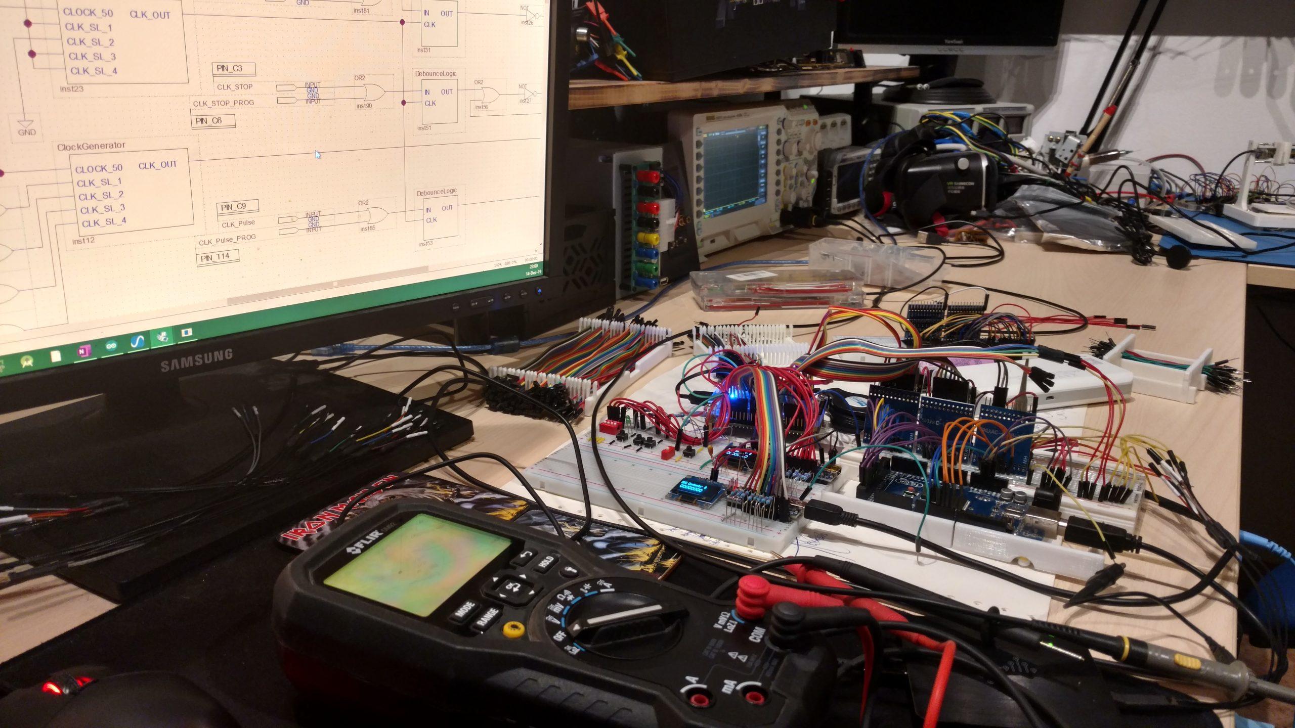
Digital Logic Design
The digital logic was designed in Quartus. This is an IDE made by Intel for “programming” the Altera FPGAs(The DE0 Nano development board has an Altera Cyclone IV FPGA on it.).

When it comes to making digital logic designs in Quartus you can either use HDL(hardware definition language) or discrete logic gates and premade logic blocks like flipflops, multiplexers, counters, … Or you can use a combination of both, which is what is most commonly done. See this post I made for more information about Quartus and an example of Verilog HDL. As I have mentioned before I decided not to use HDL or any premade logic(I only used premade logic blocks after I already made a similar component before.).
Here you can see the top level design of the whole computer. However in this post I won’t go over the construction of every component. If you are interseted in that see the section with links to indivinual post bellow.
Some Differences compared to a Breadboard computer
Unlike with a breadboard computer where you would use DIP TTL logic chips for the RAM, ALU, Registers, … I had the ability to make all the components from scratch. Here are some of the most notable differences:
- Instead of using DIP switches for programming, my computer has an Arduino interface with an app on the PC(This could actually be used with a breadboard computer too.).
- Everything is assembled from scratch. For example, flip-flops, which then make registers that in turn are used to make the RAM, the program counter was made by multiple ripple carry counters, …
- The RAM and the control unit use a decoder built from scratch. In contrast, Ben used an EEPROM to do the instruction decoding which is a great way to avoid having a mess of wires on the breadboard. For me, however, it was easier to just implement the decoder logic.
- Instead of using 7 segment displays and LEDs to display the output register and bus content, I used an Arduino with an OLED display is used.
- The clock is taken from a 50MHz crystal oscillator present on the FPGA dev. board. It is then divided using a PLL to get a lower frequency. Finally, I then use daisy-chained ripple-carry counters to perform the final frequency division. I then tap off the different frequencies from the different outputs of the ripple carry counters.
Programming
To make programming the computer easier I made this “IDE”. In the first code editor, you write your assembly. In the second one, the machine code gets generated. And in the third one, you can define your assembly(map the assembly to machine code). You can also save/load your assembly program and your assembly definition.
On the left, you have the controls column. At the very top, you can establish a COM port connection to the Arduino.
Then you have the option to set your RAM size, RAM word length, and the memory address length. Currently, this is fixed and can’t be changed. I didn’t really need the option for a bigger memory so I skipped implementing this feature(might add it in the future).
Finally, there are the controls that allow you to control the computer straight from the application/”IDE” on the PC. These controls have the same functionality as the ones on the breadboard.
Programming the computer this way is much faster and easier than using dip switches and manually setting the contents of each RAM address. Especially when I was debugging something and the FPGA had to be reconfigured meaning the computer lost everything in RAM.
See more info about the Arduino programmer here(code and how it works in more detail).
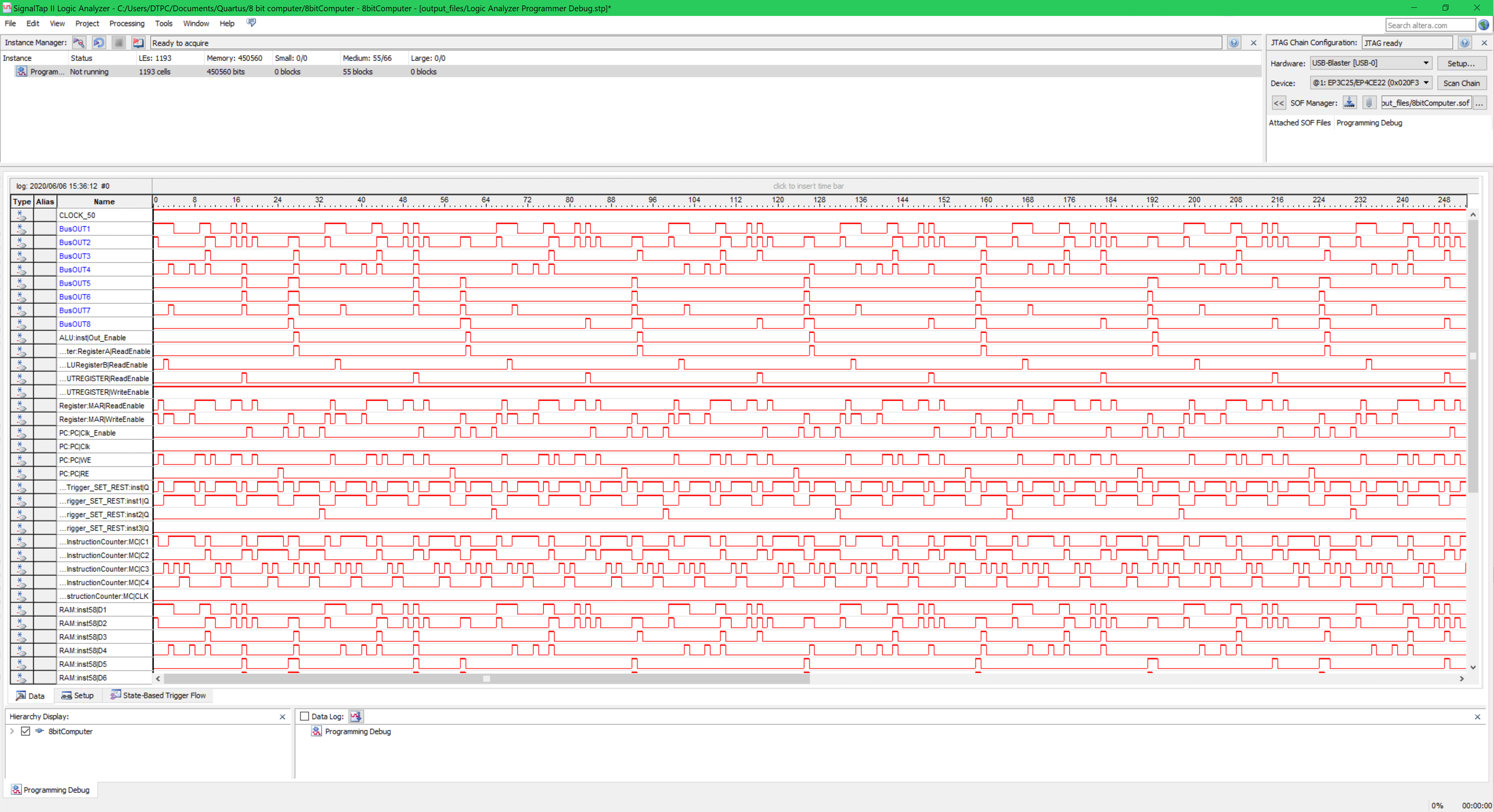
Debugging The Designs In The FPGA
The debugging can be a bit difficult in an FPGA compared to a breadboard where you can just use a multimeter/oscilloscope to probe your signals anywhere and at anytime. With the FPGA you have to connect the point you want to monitor to a pin first, re-compile, reprogram the FPGA and then you can measure the value. However, Quartus does have a very useful tool called signal tap logic analyzer. This is a logic analyzer that gets embedded in your FPGA(it will occupy some space) and provides you with the values in the Quartus IDE.
Demonstration
Topics In More Detail
This post was a general overview of the 8-bit FPGA computer. Here you can find links to posts about a specific topic or component of the computer.
Build Progress