In this post, we’ll take a look at the flip-flop which is one of the most common and essential logic blocks used in digital logic design. It can be used used for lots of different things. If you take a look at my 8-bit computer build you will see that flip-flops are used all over the place.
You can use premade flip-flops provided in Quartus. However, I wanted to build my own from scratch to truly understand how they work.
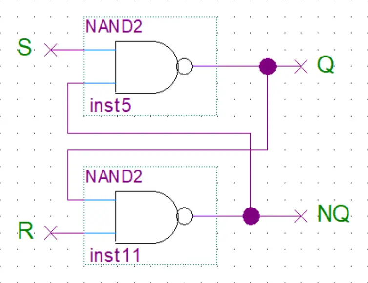
NAND Gate SR Latch
But before building a flip-flop let’s look at the most essential element required to make one: the SR latch.
SR latches are most commonly made from NAND or NOR gates. It doesn’t really matter what you use but I will stick with using NAND gates.
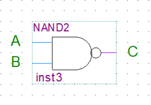
NAND Gate
NAND Gate Truth Table
A
B
C
0
0
1
0
1
1
1
0
1
1
1
0
Now assuming you know the behavior/truth table of NAND gates we can explore how they can form a latching circuit that can store state. This is achieved by connecting the outputs of each gate one of the inputs of the other gate.
SR Latch
SR Latch Truth Table
S
R
Q
NQ
0
0
/
/
0
1
0
1
1
0
1
0
1
1
0
0
The S(set) input can be toggled to set Q to high or the R(reset) can be toggled to set Q low.
Below you can play around with the circuit yourself to see how it works. I think that this will be way more intuitive and easy to understand compared to me describing it with words.
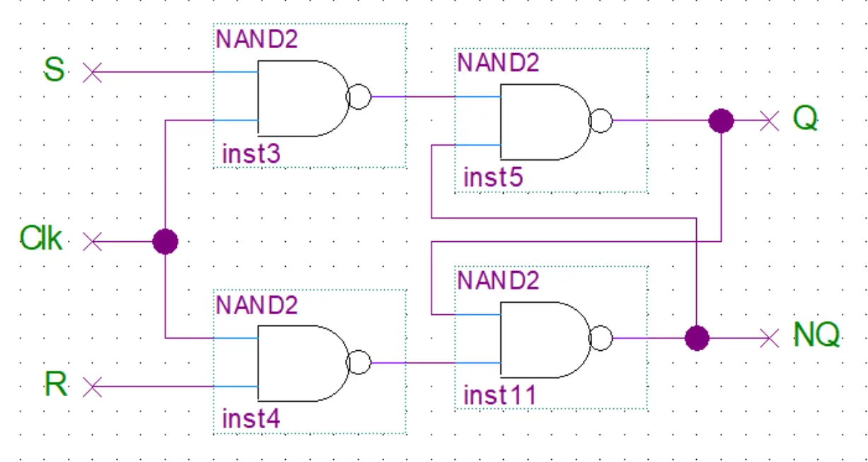
Clocked SR Flip Flop
The SR latch will change state whenever the inputs change. But we want the state to change only on a certain condition like when the clock signal is present. To accomplish this we add a NAND gate to the S and R inputs. Then we tie together the inputs of those gates and use that as an input for the clock signal. While the other two outputs now become the S and R. Now the set/reset will only be possible while the clock signal is present.
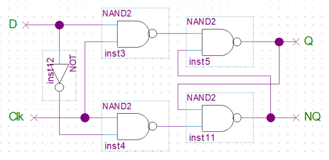
D Flip Flop
The SR flip-flop still has two inputs(S,R) that require to be toggled separately to change the latched value from 0 to 1 or vice versa. We wouldn’t be able to store the value from a single dateline this way. What we want is a single input to which we can connect our data line. Then when the clock signal is present the value from the data line(0 or 1) gets stored in the latch.
This can simply be done by connecting the S input to the R input through a NOT gate.
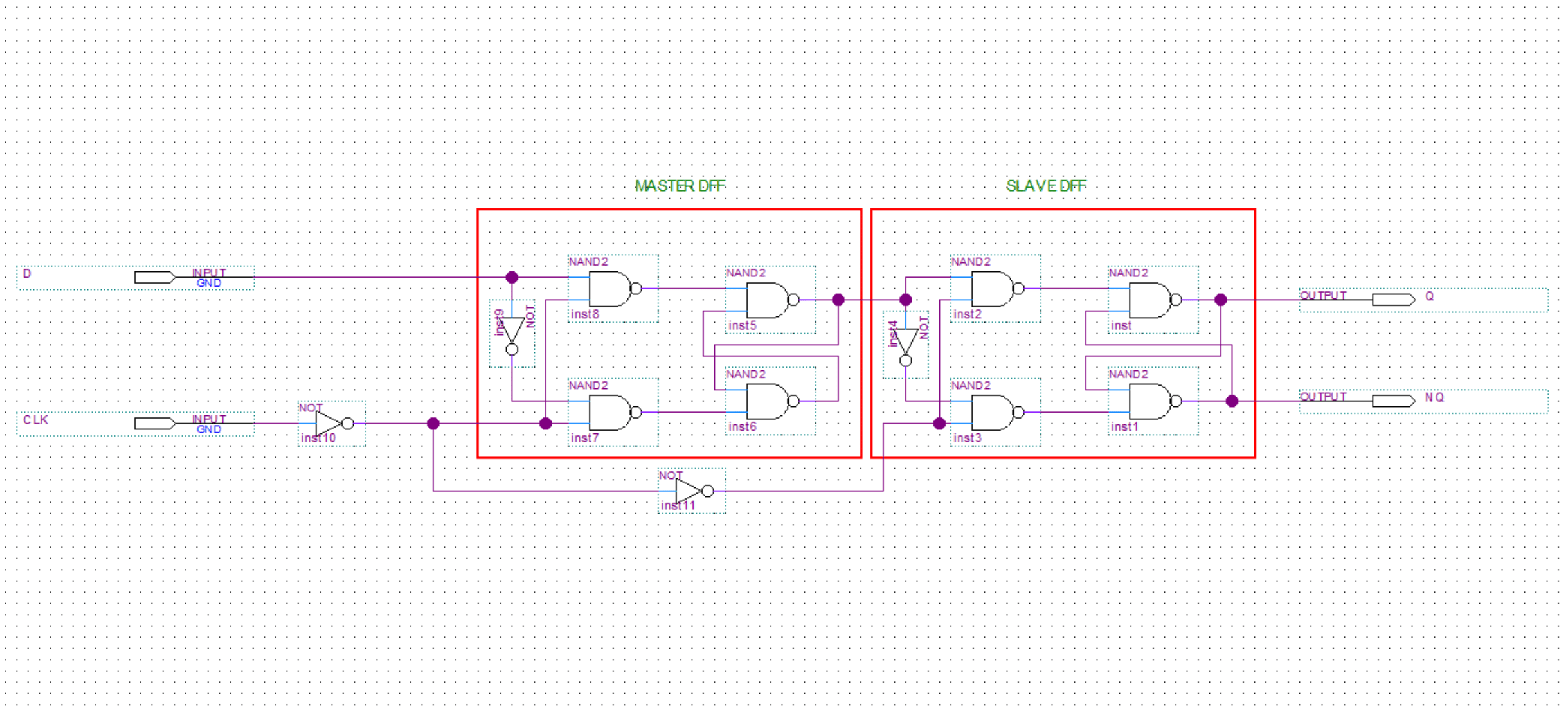
Master Slave D Flip Flop
After making our D flip-flop we now stumble upon another problem. We only want the data to be read into our flip flop on the rising edge of the clock. If the signal changes after the rising edge of the clock we don’t want the change to be registered. To do that we can attach two D flip-flops one after another in a master-slave configuration(see below).
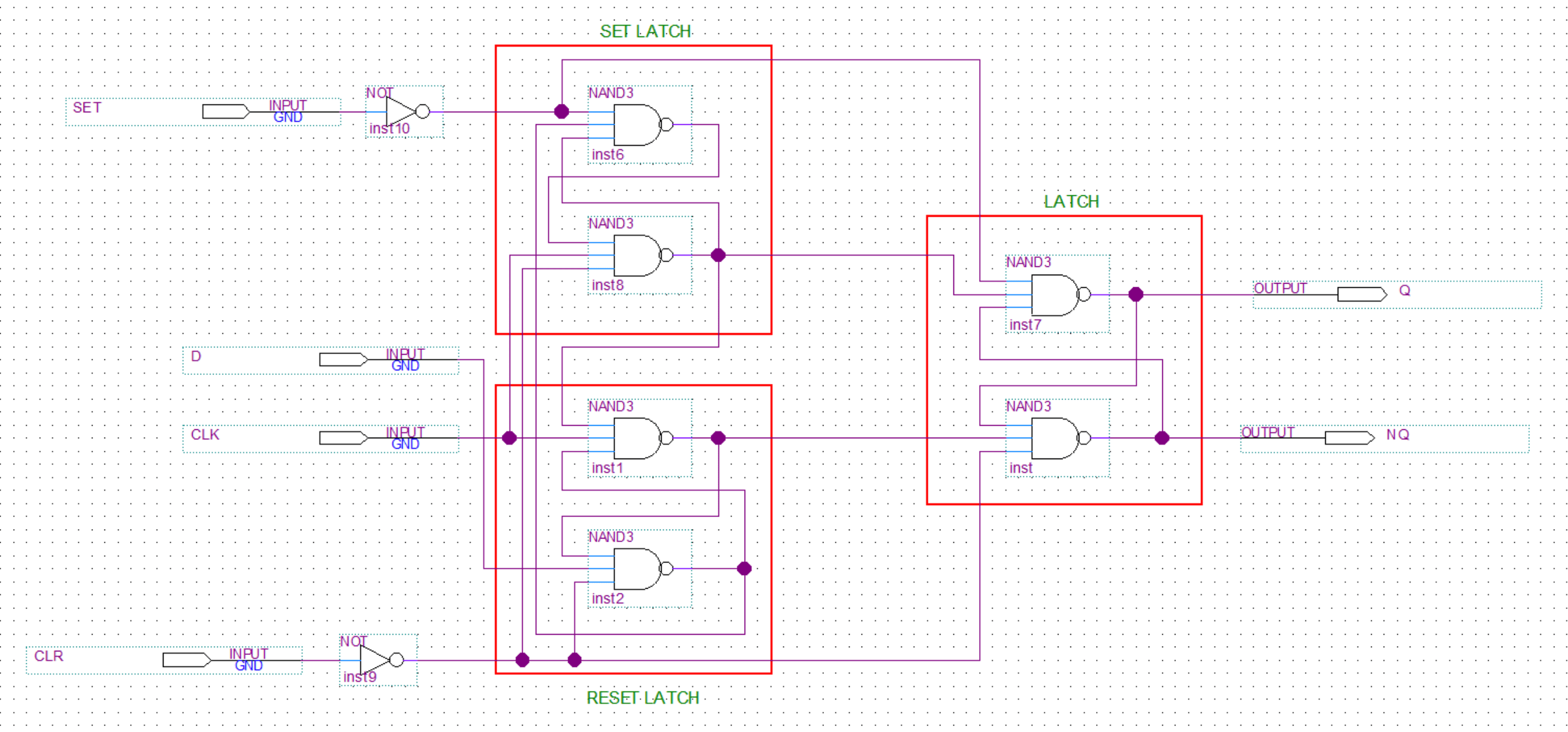
Edge Triggered D Flip Flop with Asynchronous Set and Reset
Ok, almost done now. The last thing we need to add is an asynchronous set/reset. This will be useful when resetting our computer as we can simply apply a 1 to the reset/clear input and the flip-flop Q output will reset to 0 without having to wait for the clock hence why it’s called asynchronous.
The design is a bit different here, you can see three latches. One to latch the set signal, one to latch the reset signal, and the final latch that stores the state. The NAND gates used here have three inputs so we can feed in the additional set/reset signal.
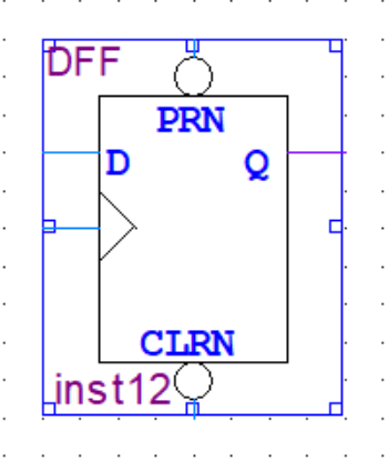
Here is a simulation of the final circuit for better understanding(but without the set and reset functionality).
Conclusion
This is how I made the flip-flops I used in my 8-bit computer build. The simpler alternative would be to use the premade D flip-flop provided by Quartus and save yourself some time. 🙂 But hopefully, now you at least somewhat understand the inner workings of a flip-flop.
Is the Asynchronous Set and Reset DFF positive and negatively edge triggered? (I noticed this when I replicated the schematics linked in the article). Or is it mean to be positively edge triggered only.


Is the Asynchronous Set and Reset DFF positive and negatively edge triggered? (I noticed this when I replicated the schematics linked in the article). Or is it mean to be positively edge triggered only.
Hi.
It is positive/rising edge triggered. If you want to change that you can simply put a NOT gate before the clock input.
HI, can you please help me for getting aware about the software you are using for simulation ?
Hi, you can find it here: https://falstad.com/circuit/circuitjs.html
And if you want the source code: https://github.com/SEVA77/circuitjs1