8-Bit Computer RAM

RAM
Share:

About

In this post, I will describe how I implemented the RAM in my 8-bit computer

The RAM size is very small, 16 cells(words) each one with 8 bits. It’s a small and simple computer so a program and its variables will be directly loaded into memory using a programmer. Results and any temporary variables are also all just stored in RAM. The only exception is if you want to output a value you can directly load it into the output register. 

Note: The images don’t include the whole circuits as they are too big. The circuitry just repeats anyway so you are not missing out on anything. 

MAR(memory address register)

Before a RAM read or write operation is about to be executed the memory address has to be stored into the MAR. Then when the read or write is performed the MAR will provide the RAM with the memory address location.

RAM(random access memory)

The RAM is connected to the bus via 8 inputs and 8 outputs(one for every bit of the 8-bit computer). The clock, read and the data inputs all have two possible sources. One is from the computer itself while the other is from the Arduino programmer that will put the data into the RAM.
The RAM module will take in the signals to read from RAM, write into RAM, and memory address location. It also takes in the clock signal and the clear memory signal which get forwarded to the RAM cells module. The memory address first gets decoded using a decoder. Then we determine whether to read or write to that address. Finally, the signal gets sent to the appropriate input on the RAM Cells module.

RAM Cells

The RAM cells are made from registers(see how the registers are made here). The clock and clear lines of all the registers are tied together. All of the inputs/outputs are connected to an input/output BUS.

Loading data into RAM

In this image you can see the RAM data input coming from the programmer. First the data lines go through some AND gates which act as an enable/disable. Before going into the RAM the inputs from the programmer and the bus are joined together using OR gates.

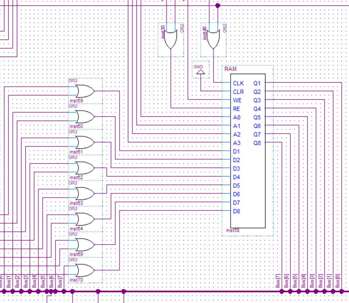
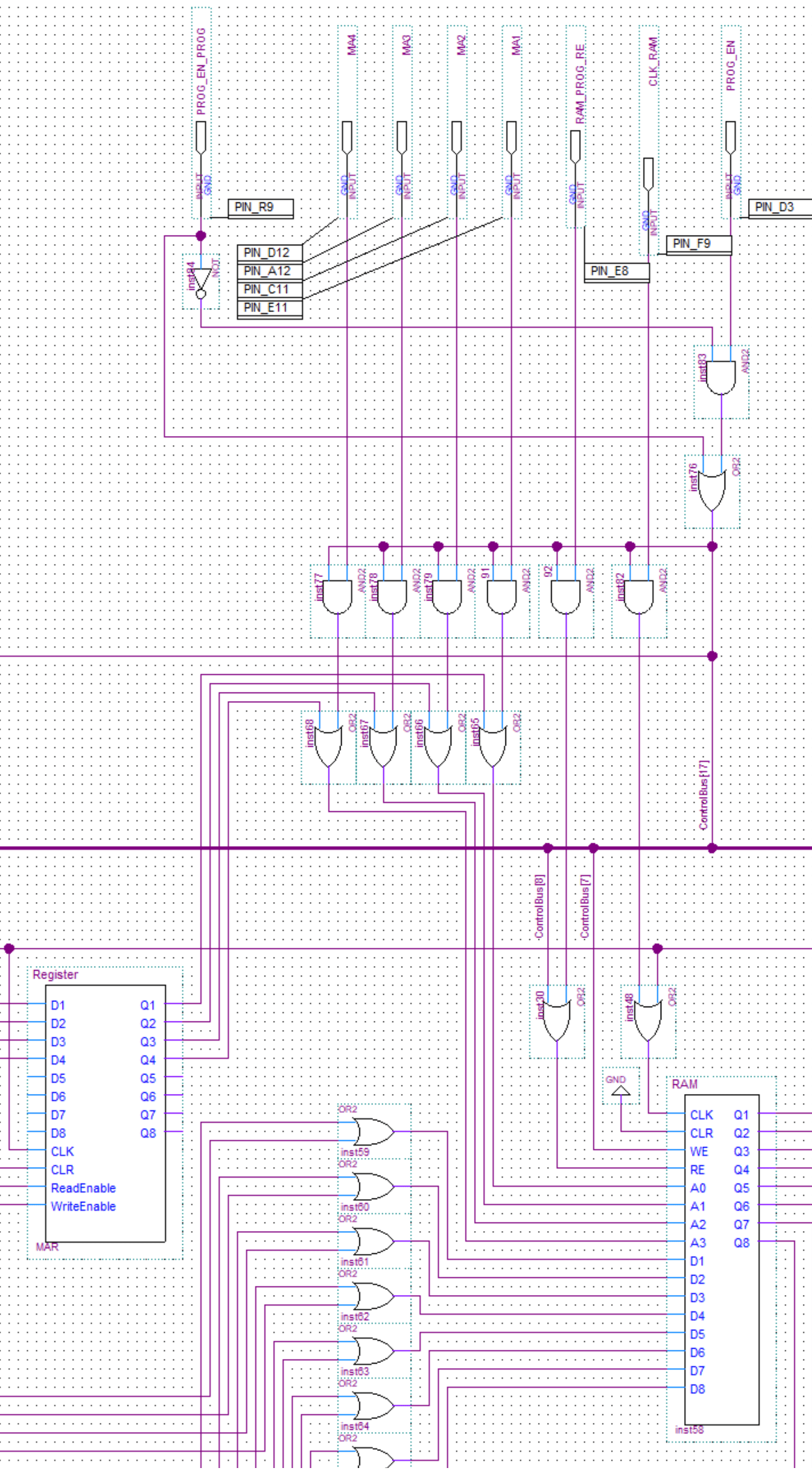
In this second image you can see  the inputs for the memory address, RAM clock, RAM read enable and program enable. Same as before all the inputs go through AND which are used to enable/disable the inputs from the programmer. Finally the inputs from the programmer and the inputs from the computer are joined using OR gates and then fed into the RAM.
Share:

Leave a Reply

Your email address will not be published. Required fields are marked *

The following GDPR rules must be read and accepted:
This form collects your name, email and content so that we can keep track of the comments placed on the website. For more info check our privacy policy where you will get more info on where, how and why we store your data.

Advertisment ad adsense adlogger