This tutorial will cover the hardware and software setup for the MAX II EPM240 CPLD. We will also make a simple logic design in Quartus to upload to the CPLD.
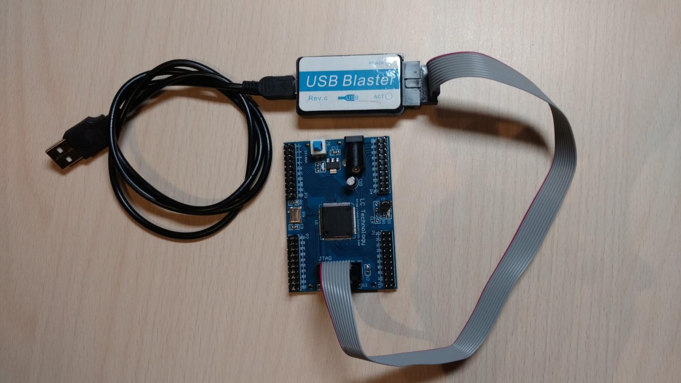
This little dev board can be picked up on eBay or Aliexpress for around 10 bucks(including the USB blaster). It’s cheap, easy and simple compared to some of the other FPGA dev boards. Despite that, I didn’t find a lot of tutorials and projects(compared to the Arduino stuff) with this board so I thought I’d make a tutorial.
First, you will have to download and install Quartus 13.1 (there are other versions that support the MAX II CPLD but I will be using 13.1).
You can find Quartus 13.1 web edition here on Intels website but you will have to make an account and register as a company to be able to download the software(apparently you can just make up a company as they don’t really check).
Alternatively, you can go on pirate bay, search for Quartus 13.1 web edition and download it from there.
After having downloaded Quartus go ahead and install it. I am not going to cover the installation here as it’s just like installing any other program. Check all the boxes, agree to everything, click next without reading, … you know the drill ;).
Hardware setup
Connect the USB blaster to your computer. I believe that any drivers should get installed automatically so you don’t have to worry about that. If they don’t you can perform a manual install:
Connect the programmer, open device manager, find your device, open the properties and select the driver tab, click update driver, “Browse my computer for drivers” and select the “path to Quartus installation”\quartus\drivers\
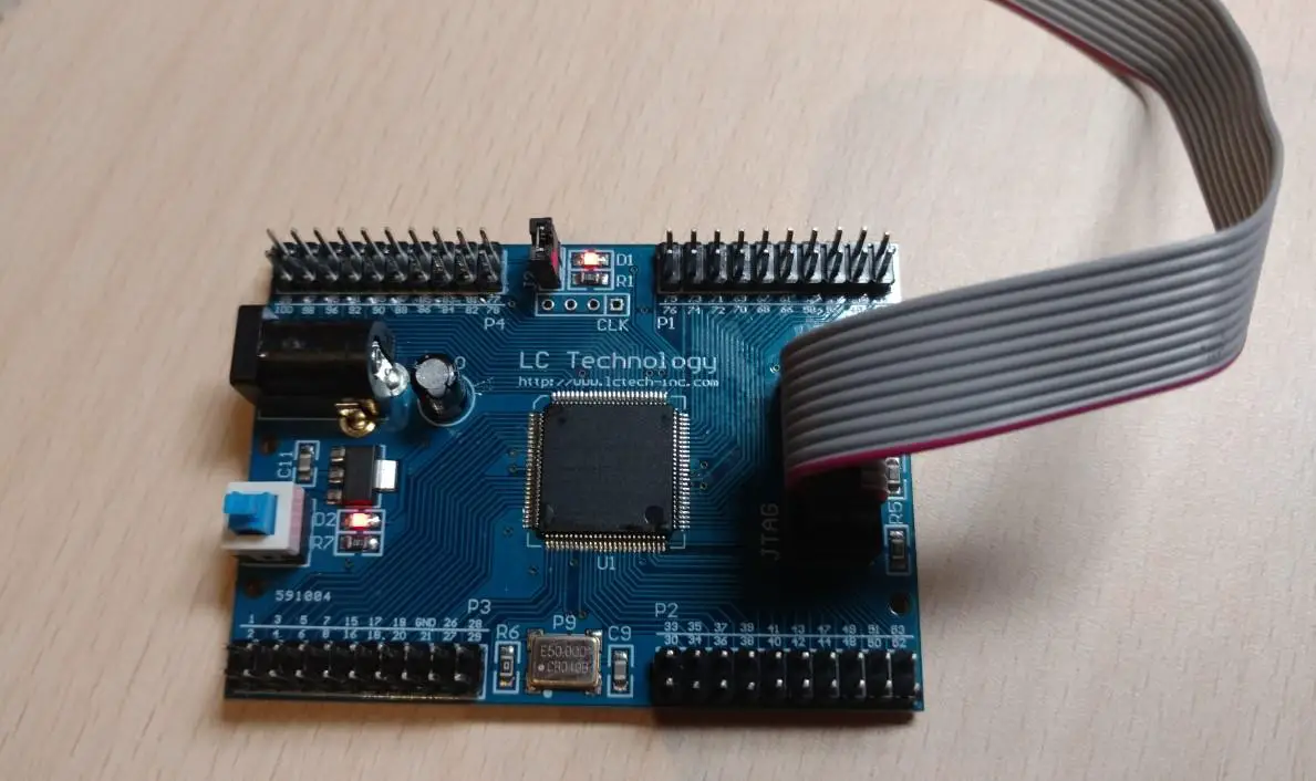
Next, connect the ribbon JTAG cable from the USB blaster to the development board.
Usually, the CPLD will already have a blink “program” uploaded to it, so you should see the top LED starting to blink. The bottom left one is the power indicator LED.
Logic design
Making a project
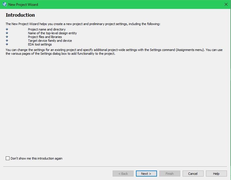
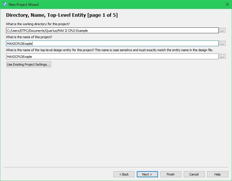
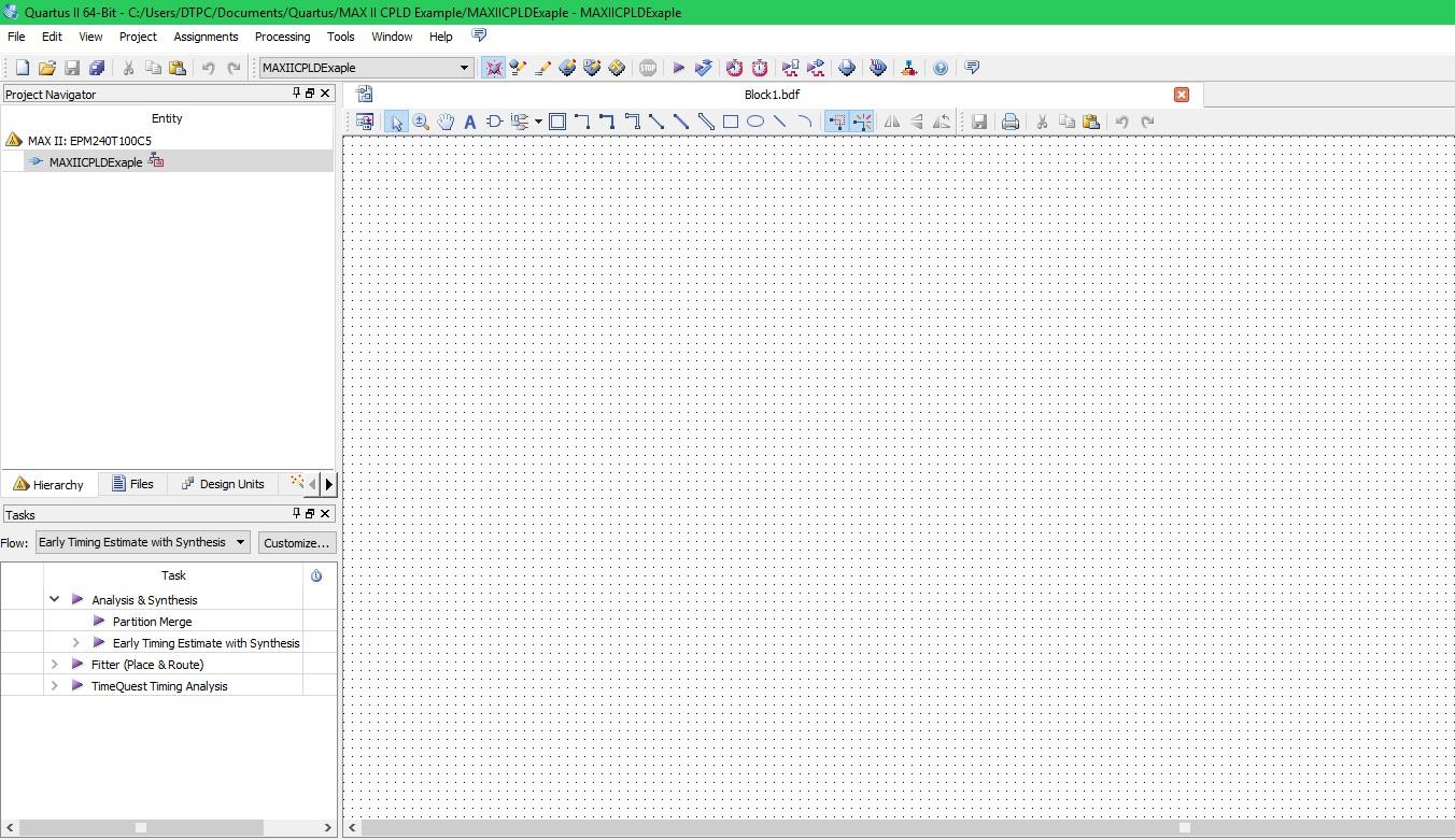
First, open up Quartus and start a new project using the project wizard.
Click next.
Name your project and set the path to where you want to save it then click next.
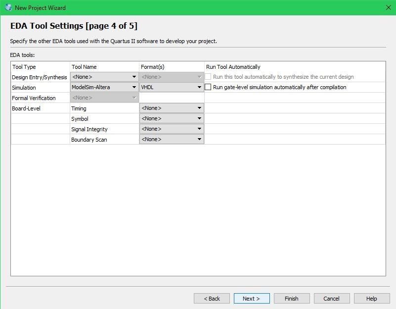
Just skip this one and click next.
Select the MAX II Device family. Under Available devices select the CPLD that you have on your board. In my case, it’s the EPM204T100C5. If you are using the same development board it should(to be sure you can just look at what it says on the chip) be the same for you.
Just click next.
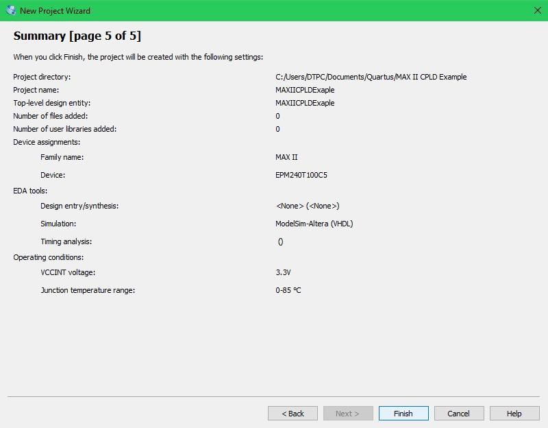
Click finish and we are all done with creating our project.
Making a design
We are going to make the “Hello World!” of digital electronics. A really basic logic design that will blink an LED.
We will take the onboard clock(2 MHz) and lower it’s frequency down to something the human eye can actually perceive as blinking. We will achieve this using a counter that will act as a frequency divider. The counter will be implemented in Verilog HDL. Then we will output the signal to the onboard LED.
Add a new .bdf file: File > New > Design Files > Block Diagram/Schematic File.
Open the newly added file(on the left side in the project navigator). This is going to be our main design file where we implement all the functionality.
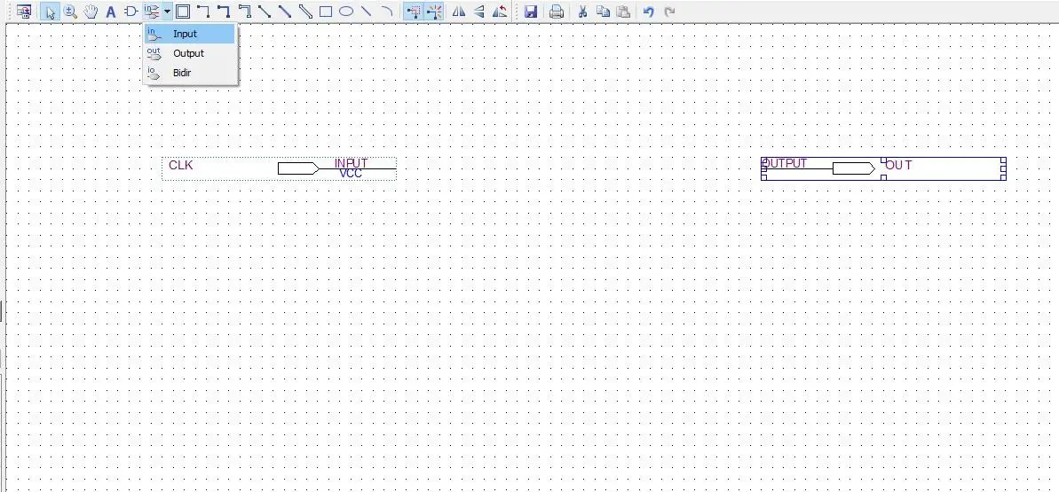
Let’s add an input and name it CLK as this input will get connected to the onboard(on the actual board not in the CPLD) clock. Let’s also add an output named OUT.
In Quartus, we have the option to either draw out discrete logic gates and connect them together or use HDL(hardware definition language). HDL files can be made into “logic block” symbols. These logic blocks can then be used the same way as symbols.
To create the counter in Verilog first add a new Verilog HDL file like so: select File > New > Verilog HDL(similar to adding the .bfd file before). After that paste in the following code:
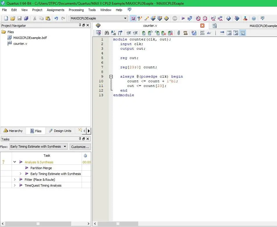
module counter(clk, out);
	input clk;
	output out;

	reg out;

	reg[23:0] count;

	always @(posedge clk) begin
	   count <= count + 1'b1;
	   out <= count[23];
	end
endmodule
This is what you should have now. I won’t go into details about Verilog in this post, but the code above makes a counter that can be used for a frequency divider. For now, you don’t have to understand it. We just want to get the LED blinking.
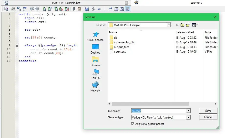
Save the Verilog file by: File > Save As.
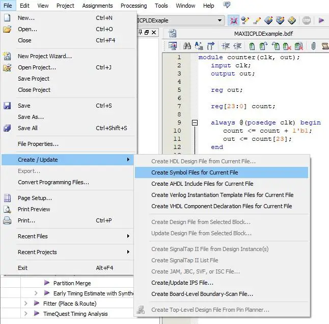
Now we need to make a logic block symbol out of our Verilog code. Select File > Create/Update > Create Symbol Files for Current File.
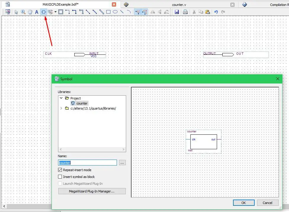
Switch back to the main file and click the add symbol button. Open the project folder and there you should see the counter symbol we have just created. Select it and add it to the main file.
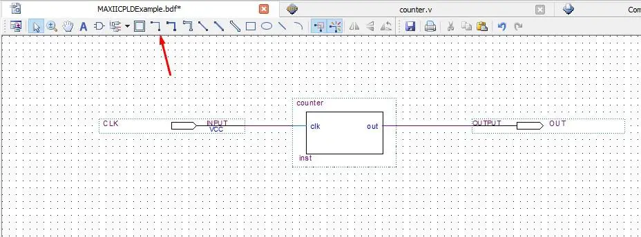
Connect the CLK input to the counter clk input and connect the counter out to the OUT output. This can be done using the line tool.
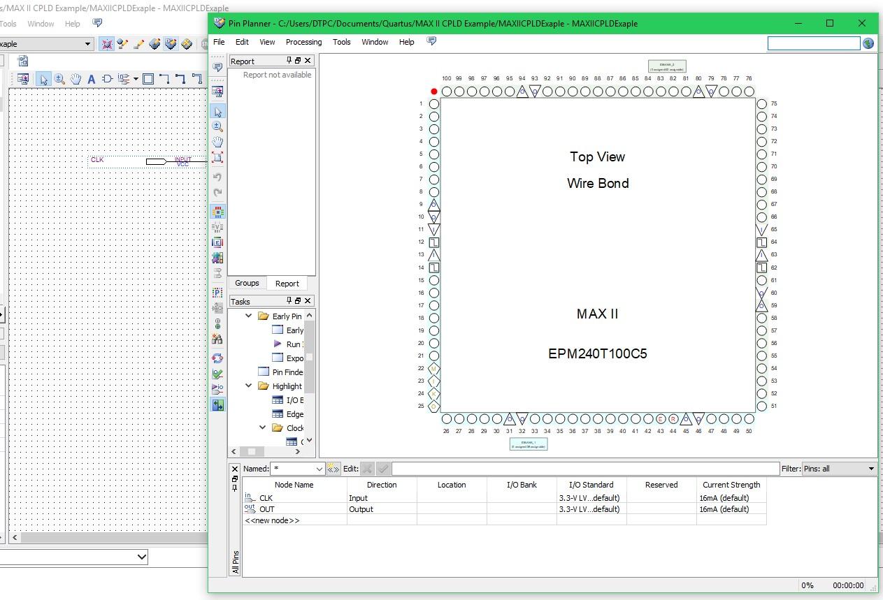
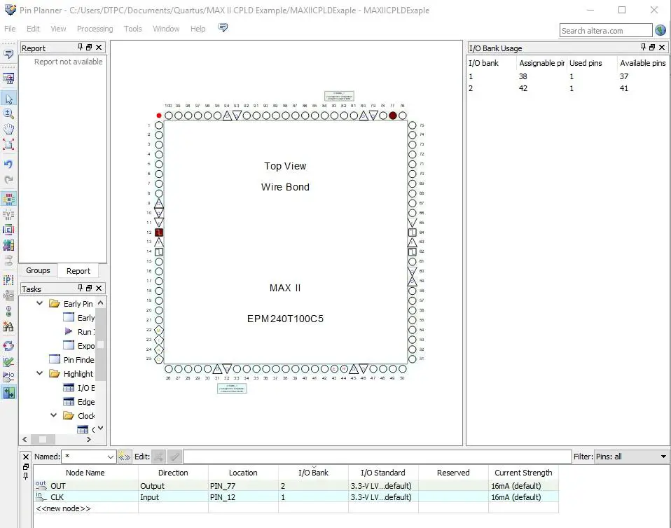
OK, great we are all done with the design itself. What we have to do now is assign the input and output to actual pins. This can be done using the pin planner tool.
Click on the location cell of the CLK input and write PIN_12 this pin has a clock signal connected to it on the development board. For the OUT output write PIN_77 which is the pin that connects to the onboard LED.
Note: If the inputs aren’t visible under Node Name column compile the project(by pressing the play button in the toolbar).
The pins are now assigned and you can also see them graphically represented on the picture above. The pin planner can now be closed.
Note: The pin numbering in the pin planner directly corresponds to the pin numbering on the development board.
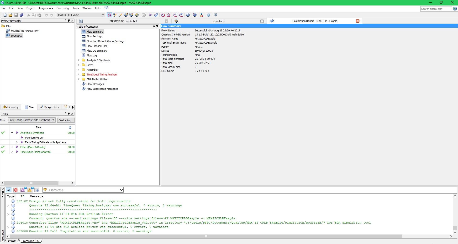
Next, the project has to be compiled to a bitstream(.sof file). This can be done by pressing the play button in the toolbar.
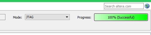
Success!
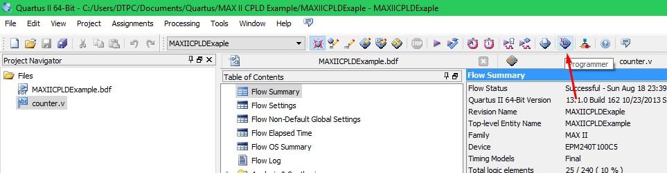
Now all that is left to do is to program the CPLD. To do so open up the programmer.
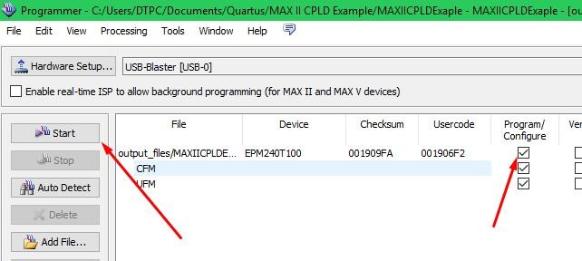
Once the programmer opens click hardware setup and selects the USB-Blaster. When you have highlighted/selected your USB blaster you can close the window.
Tick the first box under Program/Configure and press Start to program your board.
“Successful programming” and FINALLY!!!! we are done. The LED on your board should now be blinking.
Result
The output frequency can be altered by changing this line of Verilog code:
from: out<= count[23];
to: out<= count[18];
The lower number you put in the fewer times the input signal will get divided. As a result, the output frequency will be higher. You can see that in the second part of the video. The LED looks as if it’s always on because the frequency is too high. But you can see the waveform captured with a logic analyzer on the screen.
Here are some notes for the red EMP240/570 version:
// First : Provide power via barrel jack (5V from USB 2.5mm barrel jack cable – the blue version has a 2.1mm socket)
// Then : + connect USB Blaster to 10 pin JTAG socket to program it
// (Programming / autodetect fails if there’s no external power)
// clk works on pin 64 (GCLKp3) on the one I have
// There’s a visible trace to that pin, and also possibly via
// resistors / solder bridges to two outside pins on the opposite side
// out can be any general purpose pin.
// I used pin 73 – inside edge, near GND, opposite the JTAG socket, to a small LED via a 1k resistor.
// On Assignments menu, under Device > Device and pin options,
// set Reserve all unused pins to As input, tristated with weak pull-up
Thanks for this fantastic tutorial, got me up and running nicely. However in my case, I could not power the board from the USB blaster and had to provide external power.
Great writeup, hope the rest of the old tutorials get brought out of retirement (they’re still available on webarchive, fortunately)
Windows 10: I went straight to the latest version of Quartis, v20, and used manual driver installation using the file that’s available for download on the page linked for manual instruction. The drivers installed with v20 did not work with my pic-based usb blaster, but the file available here worked perfectly https://www.terasic.com.tw/wiki/File:Usb_blaster_q16.1.zip just follow the manual installation instructions, but instead of going to the Quartus installation go to the directory you extracted that zip file to. Success! Quartus 20 sees the usb blaster, and programs just fine!
A number of things here: I was unable to get Quartus to recognise the programmer (WIN 7/64) & (WIN 10/64) – unable to download a 32 bit version to try on an alternate (32 bit) machine. Eventually using UBUNTU I was able to get the USBlaster recognised by the PC but attempts to program the device ended with the Progress (Failed) – although the blue program? light did light the device after 6 days still only flashes a red LED….. If there’s any one left alive trying this who can help.. Seriously the blurb above was extremely useful – clearly the cavaet is ‘the driver should load’ – this is August 21 and I’m using Quartus prime lite (free) – does it have the capability to program is my thought?.
1. Plug the USB-Blaster into your PC.
2. Open the Device and Printers (Control Panel | Devices and Printers).
3. Under Unspecified, USB Blaster should be listed. Right mouse click on this and then select Properties.
4. Select the Hardware tab and select Properties.
5. A new window should pop up with the General tab already selected. Select Change Settings.
6. Again a new window should pop up with the General tab already selected. Select Update.
7. Select Browse my computer for driver software.
8. Find “Path to Quartus installation”\quartus\drivers\
• (Note 1: Your altera file is located at the location you selected when you first installed quartus. The location listed in this document is the default location)
• (Note 2: Stop at the drivers folder, i.e., do NOT go deeper by opening a folder within the drivers folder)
1. Select OK. Make sure the proper path was selected then select Next.
2. If the Windows security window pops up Check the Always trust software from “Altera Corporation”box and select Install.
Thanks for your reply, I should have stated I followed the instructions for attempt to get it working, I had tried many times but each time windows reported a problem – so I’m using Linux which recognised and talks to the programmer, sadly there seems to be a problem with the programmer (not the human one) as at one point it did successfully program the chip, on one occasion. Since then again it responds with the QP Dialog box “Programmer operation was NOT successful, I think it’s a cheap copy and the cockroach has died.. This is all on the latest and greatest Ubuntu 64 platform 🙂 I think it’s a bin job (not the trash bin yet though)
I posted in detail above, but following manual installation instructions with this file, https://www.terasic.com.tw/wiki/File:Usb_blaster_q16.1.zip instead of the ones installed with Quartus is what it took to get it working on Windows 10 for me. My USB blaster is pic-based, but hopefully it’ll work if you have an stm32 based one. It worked fine with Quartus Prime Lite, latest version (v20 i believe).


Thanks for the tutorial!
Here are some notes for the red EMP240/570 version:
// First : Provide power via barrel jack (5V from USB 2.5mm barrel jack cable – the blue version has a 2.1mm socket)
// Then : + connect USB Blaster to 10 pin JTAG socket to program it
// (Programming / autodetect fails if there’s no external power)
// clk works on pin 64 (GCLKp3) on the one I have
// There’s a visible trace to that pin, and also possibly via
// resistors / solder bridges to two outside pins on the opposite side
// out can be any general purpose pin.
// I used pin 73 – inside edge, near GND, opposite the JTAG socket, to a small LED via a 1k resistor.
// On Assignments menu, under Device > Device and pin options,
// set Reserve all unused pins to As input, tristated with weak pull-up
Hi.
Thanks for the info.
Thanks for this fantastic tutorial, got me up and running nicely. However in my case, I could not power the board from the USB blaster and had to provide external power.
Great writeup, hope the rest of the old tutorials get brought out of retirement (they’re still available on webarchive, fortunately)
Windows 10: I went straight to the latest version of Quartis, v20, and used manual driver installation using the file that’s available for download on the page linked for manual instruction. The drivers installed with v20 did not work with my pic-based usb blaster, but the file available here worked perfectly https://www.terasic.com.tw/wiki/File:Usb_blaster_q16.1.zip just follow the manual installation instructions, but instead of going to the Quartus installation go to the directory you extracted that zip file to. Success! Quartus 20 sees the usb blaster, and programs just fine!
Thanks for sharing.
A number of things here: I was unable to get Quartus to recognise the programmer (WIN 7/64) & (WIN 10/64) – unable to download a 32 bit version to try on an alternate (32 bit) machine. Eventually using UBUNTU I was able to get the USBlaster recognised by the PC but attempts to program the device ended with the Progress (Failed) – although the blue program? light did light the device after 6 days still only flashes a red LED….. If there’s any one left alive trying this who can help.. Seriously the blurb above was extremely useful – clearly the cavaet is ‘the driver should load’ – this is August 21 and I’m using Quartus prime lite (free) – does it have the capability to program is my thought?.
Hi, the driver can be manually installed like so:
1. Plug the USB-Blaster into your PC.
2. Open the Device and Printers (Control Panel | Devices and Printers).
3. Under Unspecified, USB Blaster should be listed. Right mouse click on this and then select Properties.
4. Select the Hardware tab and select Properties.
5. A new window should pop up with the General tab already selected. Select Change Settings.
6. Again a new window should pop up with the General tab already selected. Select Update.
7. Select Browse my computer for driver software.
8. Find “Path to Quartus installation”\quartus\drivers\
• (Note 1: Your altera file is located at the location you selected when you first installed quartus. The location listed in this document is the default location)
• (Note 2: Stop at the drivers folder, i.e., do NOT go deeper by opening a folder within the drivers folder)
1. Select OK. Make sure the proper path was selected then select Next.
2. If the Windows security window pops up Check the Always trust software from “Altera Corporation”box and select Install.
source: https://www.terasic.com.tw/wiki/Altera_USB_Blaster_Driver_Installation_Instructions
Thanks for your reply, I should have stated I followed the instructions for attempt to get it working, I had tried many times but each time windows reported a problem – so I’m using Linux which recognised and talks to the programmer, sadly there seems to be a problem with the programmer (not the human one) as at one point it did successfully program the chip, on one occasion. Since then again it responds with the QP Dialog box “Programmer operation was NOT successful, I think it’s a cheap copy and the cockroach has died.. This is all on the latest and greatest Ubuntu 64 platform 🙂 I think it’s a bin job (not the trash bin yet though)
I posted in detail above, but following manual installation instructions with this file, https://www.terasic.com.tw/wiki/File:Usb_blaster_q16.1.zip instead of the ones installed with Quartus is what it took to get it working on Windows 10 for me. My USB blaster is pic-based, but hopefully it’ll work if you have an stm32 based one. It worked fine with Quartus Prime Lite, latest version (v20 i believe).
I’m about a year late with this reply, but you’ll get the Progress (Failed) error if you don’t apply external power – 5V via the barrel jack socket.
I hope you got it working.