About
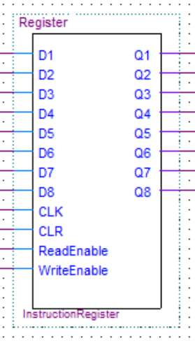
In this post, I will show how I made the registers for my 8-bit computer. I will use the flip-flops I made in this post.
And just like with the flip-flops you could use the premade register provided in Quartus. However, I wanted to build my own from scratch to truly understand how they work.
Register
Internal Design Of The Register
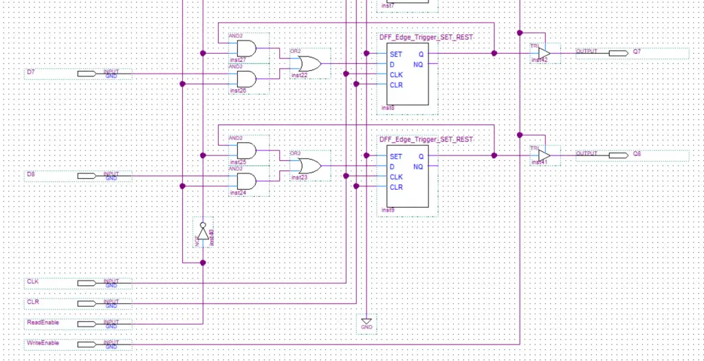
I only included the last two memory cells in the picture as the design just repeats 6 more times(once for every bit). As you can see I am using a D edge-triggered flip-flop as a memory cell to store the data.
There are tristate buffers on the outputs to control the output. Tristate buffers are used instead of AND gates because the registers might be connected to a bus. Unlike AND gates which would pull the bus low the tristate buffers will be in a state of high impedance thus not interfering with the bus.
The clock inputs are all just connected together, the same goes for the clear inputs.
Last but most definitely not least are the memory refresh circuits(two AND and one OR gate before each flip-flop). On every rising edge of the clock, the flip-flop will read in the data from the inputs. Not quite what you would want for storing data(unless you happen to be reading data in at that moment). This is why we need the refresh circuit which just feeds the output of the flip-flop back to its input unless the read enable is high. In that case, it will connect the input of the register directly to the input of the flip-flop.

